Epitaxial substrate for semiconductor element, semiconductor element, and process for producing epitaxial substrate for semiconductor element
A technology for epitaxial substrates and manufacturing methods, which is applied in semiconductor/solid-state device manufacturing, semiconductor devices, electrical components, etc., and can solve problems such as difficulties in epitaxial growth, large differences in growth temperature, and no clear implementation methods.
- Summary
- Abstract
- Description
- Claims
- Application Information
AI Technical Summary
Problems solved by technology
Method used
Image
Examples
no. 1 Embodiment approach
[0060]
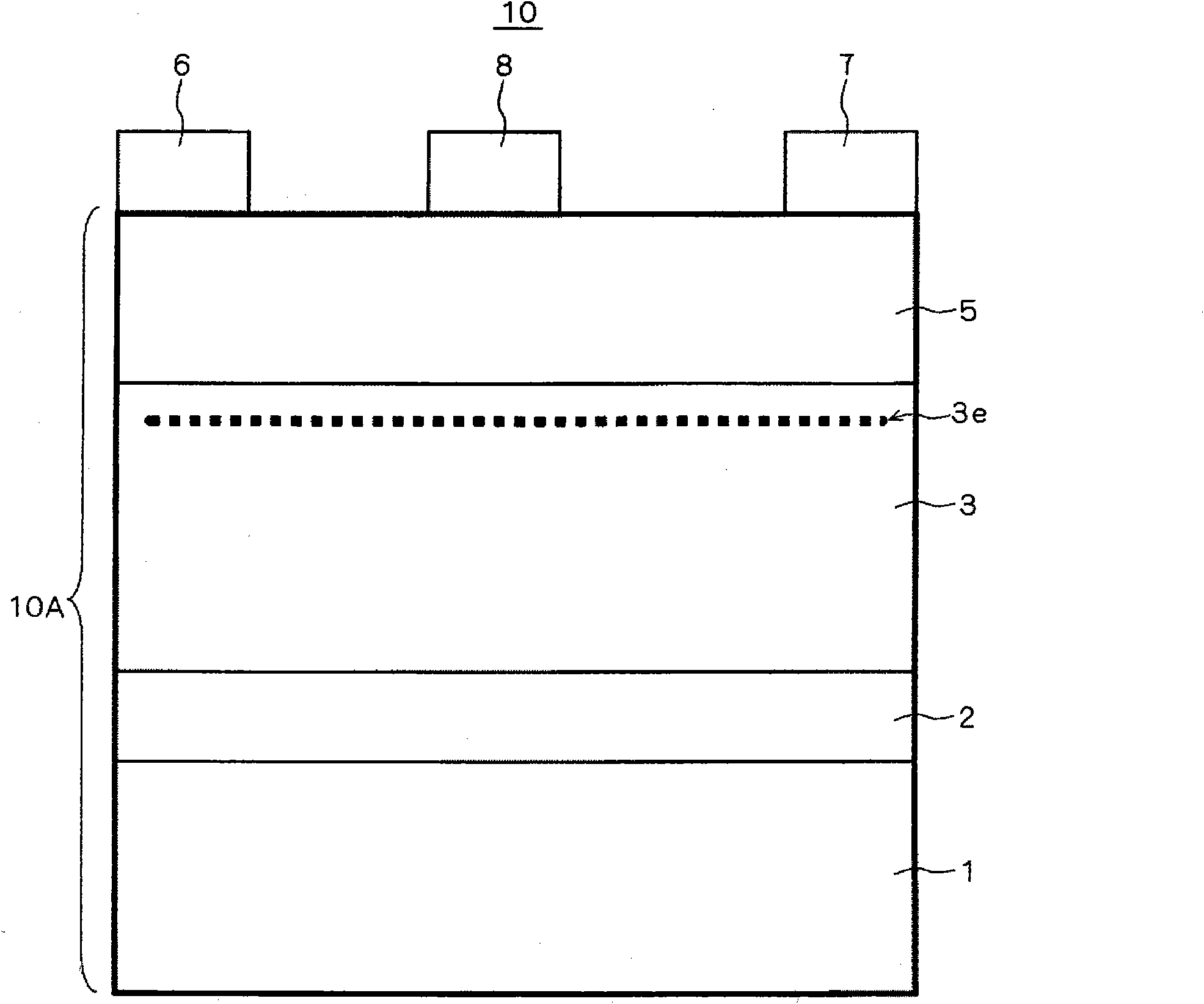
[0061] figure 1 It is a schematic cross-sectional view schematically showing the configuration of the HEMT element 10 in the first embodiment of the present invention. The HEMT element 10 has a structure in which a substrate 1 , a buffer layer 2 , a channel layer 3 , and a barrier layer 5 are stacked. It is a preferable example that the buffer layer 2 , the channel layer 3 and the barrier layer 5 are epitaxially formed by MOCVD (metal organic chemical vapor deposition) (described in detail below). Hereinafter, a laminated structure formed by laminating the substrate 1 , the buffer layer 2 , the channel layer 3 , and the barrier layer 5 is also referred to as an epitaxial substrate 10A. in addition, figure 1 The thickness ratios of the layers in the figures do not reflect actual ratios.
[0062] In the following, the formation of each layer will be described for the case of using the MOCVD method, but as long as the method can form each layer with good crystallini...
no. 2 Embodiment approach
[0116]
[0117] Figure 7 It is a schematic cross-sectional view schematically showing the configuration of the HEMT element 20 in the second embodiment of the present invention. The HEMT element 20 has a configuration in which a spacer layer 4 is inserted between the channel layer 3 and the barrier layer 5 of the HEMT element 10 in the first embodiment. Components other than the spacer layer 4 are the same as those of the HEMT element 10 in the first embodiment, so detailed description thereof will be omitted. In addition, hereinafter, the stacked structure formed by stacking the substrate 1 , the buffer layer 2 , the channel layer 3 , the spacer layer 4 , and the barrier layer 5 is also referred to as an epitaxial substrate 20A.
[0118] The isolation layer 4 is a layer formed by a group III nitride having a thickness in the range of 0.5 nm to 1.5 nm, and the total thickness of the isolation layer 4 and the barrier layer 5 is 5 nm or less. x3 Al y3 Ga z3 The N (x3+y3+z...
Embodiment 1
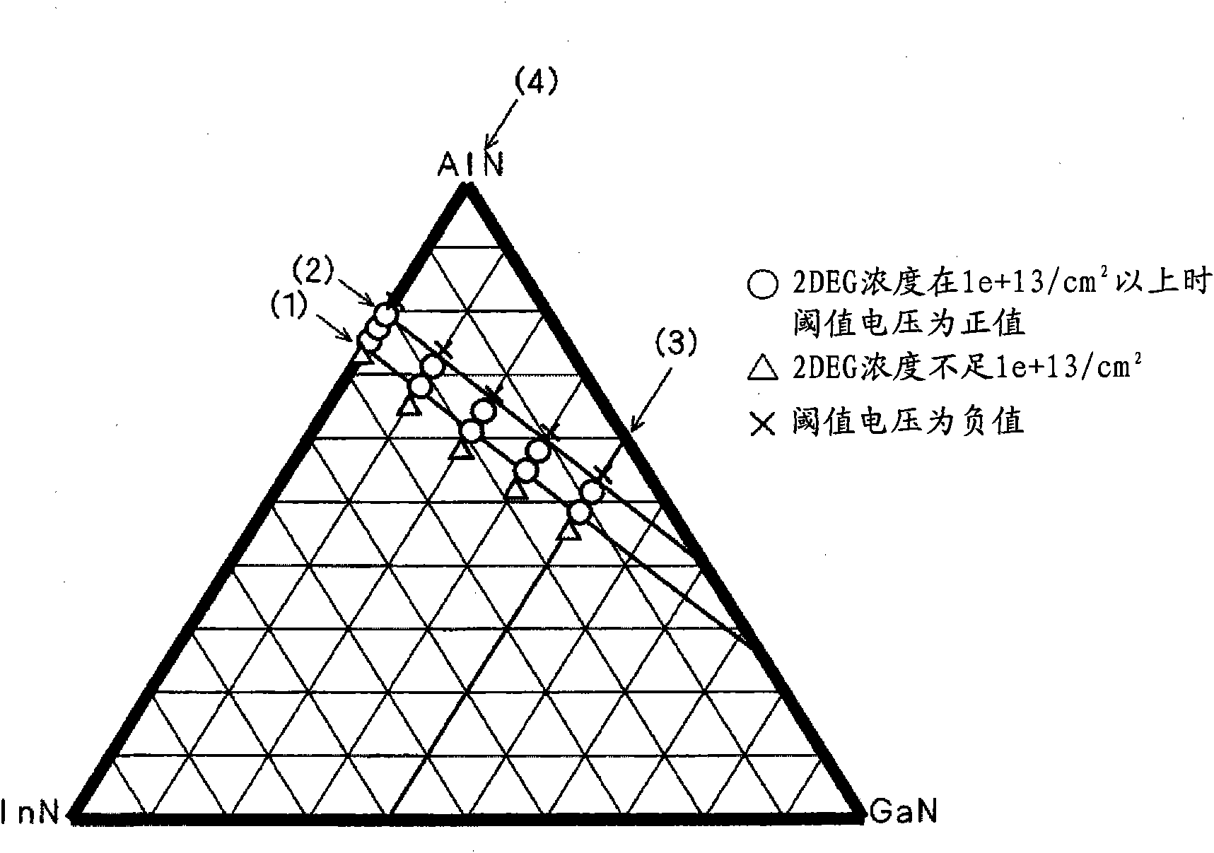
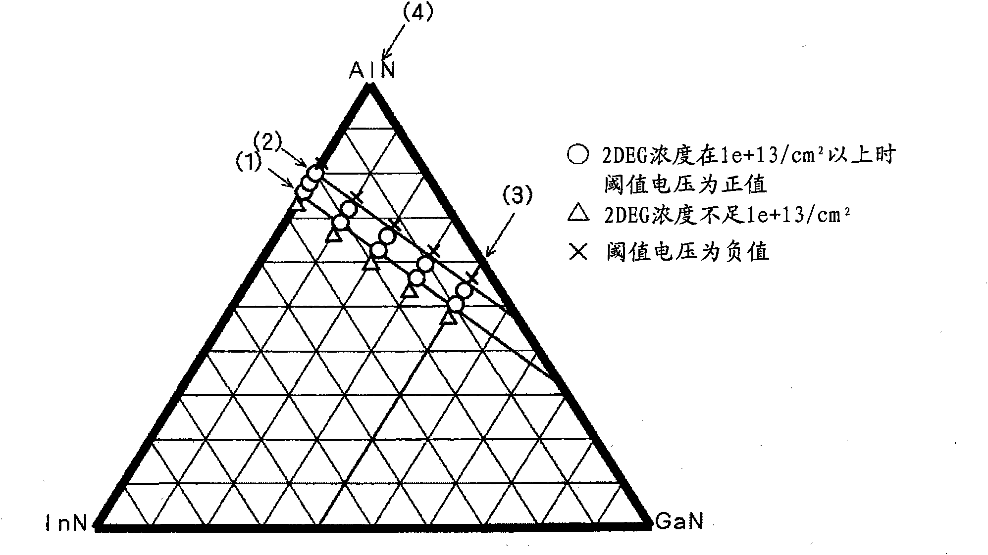
[0136] In this example, the HEMT element 10 of the first embodiment was fabricated. Specifically, a plurality of epitaxial substrates 10A having different combinations of channel layer 3 and barrier layer 5 were produced, and HEMT elements 10 were produced using them.
[0137] When fabricating the epitaxial substrate 10A, first, a plurality of 6H-SiC substrates having a diameter of 2 inches in the (0001) plane orientation were prepared as substrates 1 . Each substrate 1 was placed in the reactor of the MOCVD furnace, and after vacuum displacement, the pressure inside the reactor was set at 30 kPa to form an atmosphere gas in a hydrogen / nitrogen mixed flow state. Next, the temperature of the substrate is raised by heating the susceptor.
[0138] After the susceptor temperature reached 1050° C., Al raw material gas and ammonia gas were introduced into the reactor to form an AlN layer with a thickness of 200 nm as the buffer layer 2 .
[0139] Then, the susceptor temperature is...
PUM
| Property | Measurement | Unit |
|---|---|---|
| roughness | aaaaa | aaaaa |
| roughness | aaaaa | aaaaa |
Abstract
Description
Claims
Application Information
 - R&D
- Intellectual Property
- Life Sciences
- Materials
- Tech Scout
- Unparalleled Data Quality
- Higher Quality Content
- 60% Fewer Hallucinations
Browse by: Latest US Patents, China's latest patents, Technical Efficacy Thesaurus, Application Domain, Technology Topic, Popular Technical Reports.
© 2025 PatSnap. All rights reserved.Legal|Privacy policy|Modern Slavery Act Transparency Statement|Sitemap|About US| Contact US: help@patsnap.com


