
Formation method of contact hole

A technology of contact hole and etching stop layer, which is applied in the field of contact hole formation, can solve the problems of conductive layer 105 damage, conductive layer damage, etc., and achieve the effects of reducing damage defects, reducing damage, and increasing etching rate

Active Publication Date: 2014-03-12
SEMICONDUCTOR MANUFACTURING INTERNATIONAL (BEIJING) CORP
View PDF4 Cites 0 Cited by
  • Summary
  • Abstract
  • Description
  • Claims
  • Application Information

AI Technical Summary

Problems solved by technology

[0009] However, after testing the contact holes formed by the above method, it was found that there is a problem of damage to the underlying conductive layer. Figure 5 It is a test map of the surface of the semiconductor substrate after the contact hole is formed by using the traditional contact hole forming method
like Figure 5 As shown, there are defects caused by damage in the conductive layer 105 at the bottom of the contact hole of the semiconductor substrate

Method used


Image

  • Formation method of contact hole
  • Formation method of contact hole
  • Formation method of contact hole

Examples


Embodiment 1

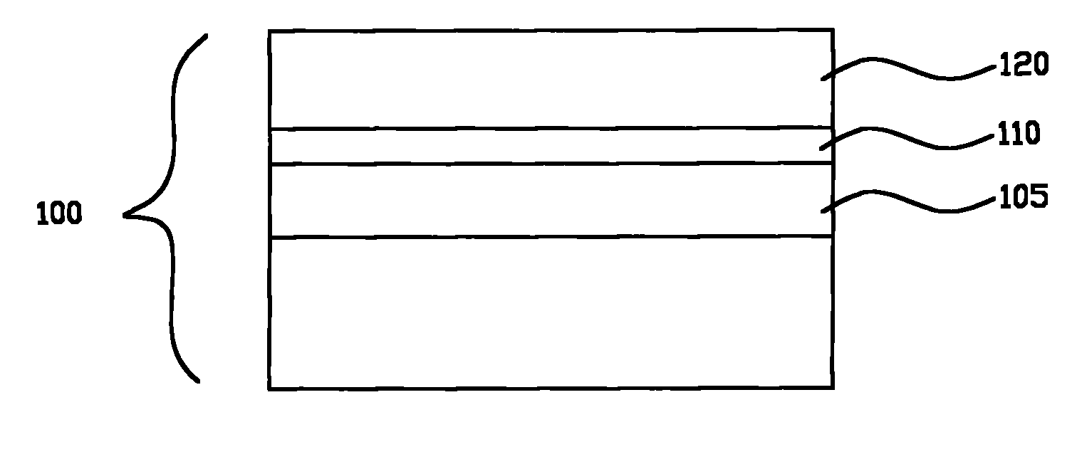
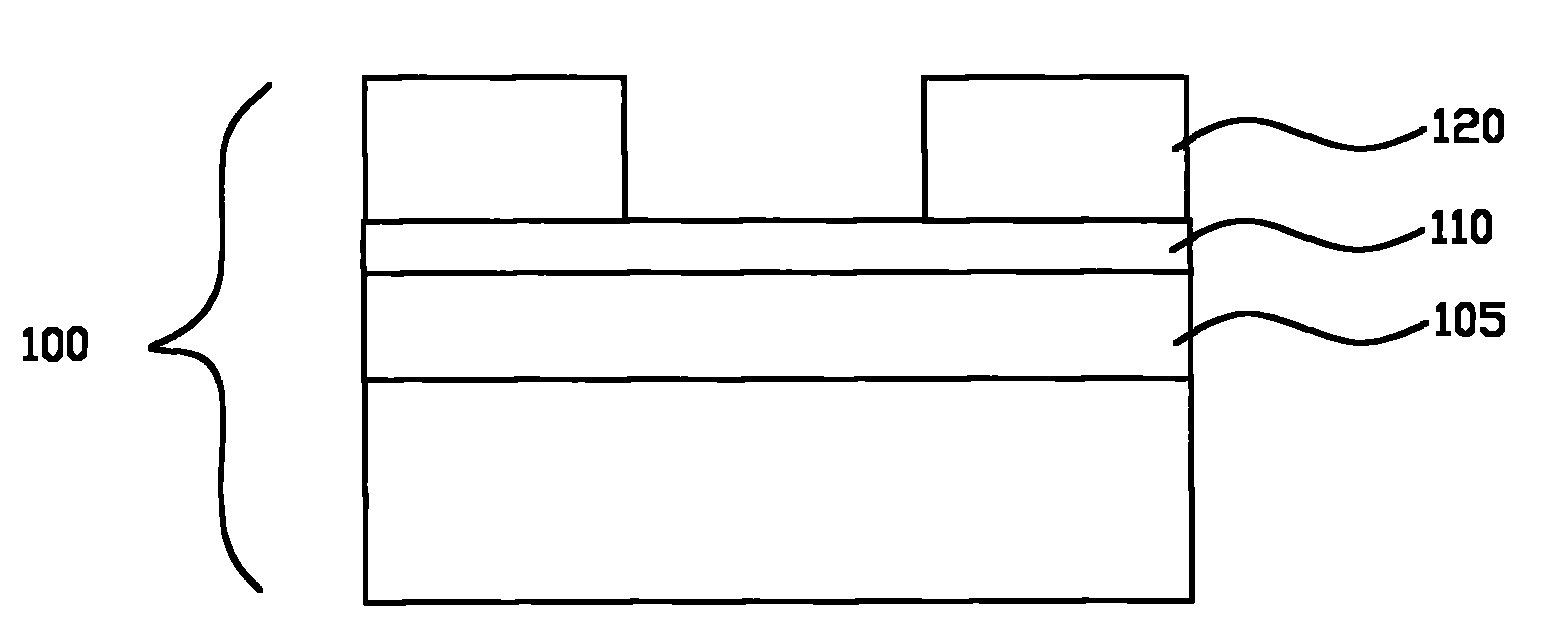
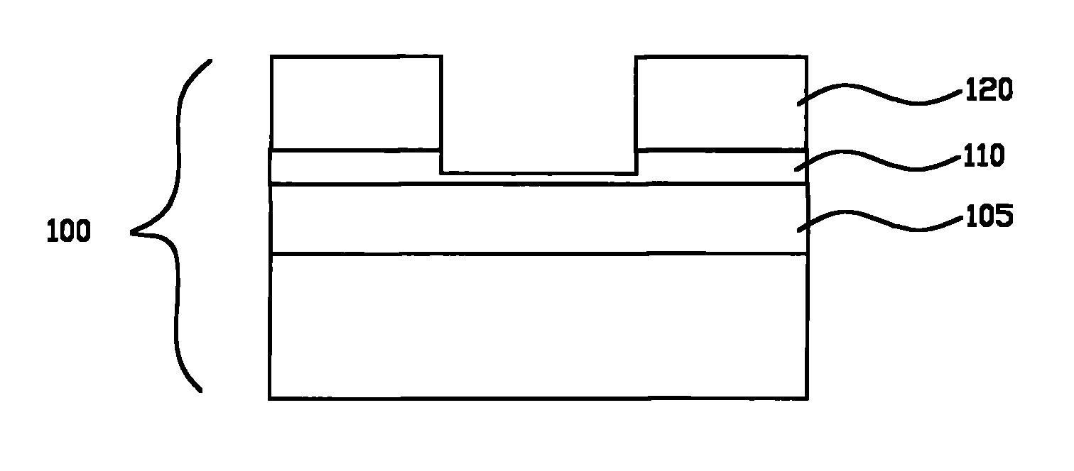
[0053] Figure 6 It is a flowchart of the method for forming a contact hole of the present invention; Figure 7 to Figure 9 It is a schematic diagram of the method for forming a contact hole of the present invention. Refer below Figure 6-Figure 9 The method of forming a contact hole according to the present invention will be described.

[0054] S110: Provide a semiconductor substrate, which includes a conductive layer, an etching stop layer on the conductive layer, and an interlayer dielectric layer on the etching stop layer.

[0055] Specifically, refer to Figure 7 , providing a semiconductor substrate 100, the semiconductor substrate 100 can be a single crystal, polycrystalline or amorphous silicon (Si) or silicon germanium (SiGe) structure; it can also be a mixed semiconductor structure, such as silicon carbide, gallium arsenide, phosphorus Gallium nitride, indium antimonide, indium phosphide, indium arsenide, or gallium antimonide; a structure with a semiconductor ma...


PUM


Abstract

The invention provides a formation method of a contact hole, comprising the following steps: providing a semiconductor substrate which comprises a conducting layer, an etch stop layer on the conducting layer and an interlayer dielectric layer on the etch stop layer; carrying out primary etching on the interlayer dielectric layer so as to form through holes on the interlayer dielectric layer; and carrying out secondary etching on the etch stop layer so as to form through holes on the etch stop layer, wherein the etching gas for the secondary etching comprises CH2F2, O2, N2 and gas with the fluorine-to-carbon ratio higher than 2. The formation method of the contact hole reduces the damage to the conducting layer at the bottom part of the contact hole of the semiconductor substrate.

Description

technical field [0001] The invention relates to the technical field of semiconductor manufacturing, in particular to a method for forming a contact hole. Background technique [0002] The manufacture of semiconductor integrated circuits is an extremely complex process, the purpose of which is to reduce the various electronic components and circuits required for a specific circuit on a small-area wafer. Wherein, each component must be electrically connected by an appropriate interconnection wire, so as to exert the desired function. [0003] As the production of integrated circuits develops toward ultra-large-scale integrated circuits (ULSI), the internal circuit density is increasing. As the number of components contained in the chip continues to increase, the available space for surface wiring is actually reduced. The solution to this problem is to adopt a multi-layer metal wire design, and use a multi-layer connection in which a multi-layer insulating layer and a conducti...

Claims


Application Information

Patent Timeline
Patent Type & Authority Patents(China)
IPC IPC(8): H01L21/768H01L21/311
Inventor 张海洋王新鹏符雅丽
Owner SEMICONDUCTOR MANUFACTURING INTERNATIONAL (BEIJING) CORP
Learn More