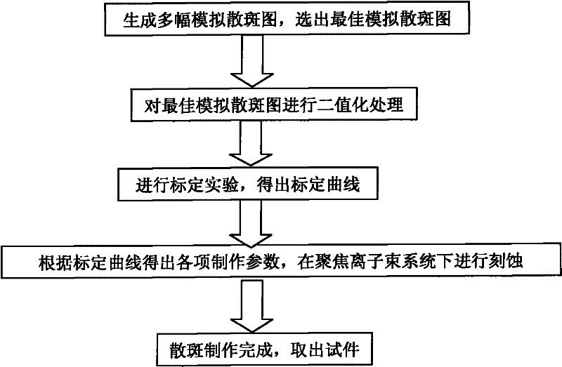
Method for making micro-nano-scale speckle
A production method and micro-nano technology, applied in the field of photomechanics, can solve the problems of complicated production process, small application range, large speckle particles, etc., and achieve the effect of simple and flexible process, no temperature requirement, and variable area
- Summary
- Abstract
- Description
- Claims
- Application Information
AI Technical Summary
Problems solved by technology
Method used
Image


Examples
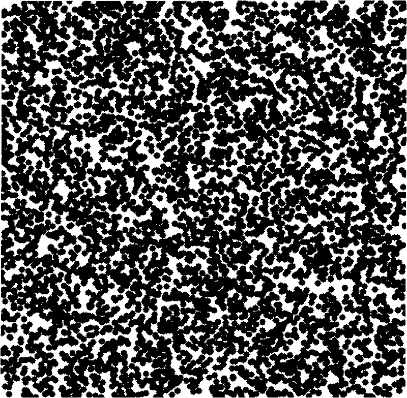
Embodiment 1
[0020] Using Matlab software to generate multiple simulated speckle images with different speckle sizes and numbers ( figure 2 ), the simulated speckle pattern is formed by the superposition of multiple speckle particles (Gaussian spots), and the gray level of each point can be expressed by the following function:
[0021] I ( x , y ) = int { Σ k = 1 s I k exp [ - ( x - x k ) 2 + ( y - ...
PUM
 Abstract
Description
Claims
Application Information
 - R&D
- Intellectual Property
- Life Sciences
- Materials
- Tech Scout
- Unparalleled Data Quality
- Higher Quality Content
- 60% Fewer Hallucinations
Browse by: Latest US Patents, China's latest patents, Technical Efficacy Thesaurus, Application Domain, Technology Topic, Popular Technical Reports.
© 2025 PatSnap. All rights reserved.Legal|Privacy policy|Modern Slavery Act Transparency Statement|Sitemap|About US| Contact US: help@patsnap.com