Amorphous silicon solar cell with three-dimensional photonic crystal serving as back reflecting layer and manufacturing method thereof
A back reflective layer and photonic crystal technology, applied in photovoltaic power generation, circuits, electrical components, etc., can solve the problems of low reflectivity of the back reflective layer and low efficiency of amorphous silicon solar cells, so as to improve photon utilization efficiency and increase light Current density, photoelectric conversion efficiency, and effect of increasing thickness
- Summary
- Abstract
- Description
- Claims
- Application Information
AI Technical Summary
Problems solved by technology
Method used
Image
Examples
specific Embodiment approach 1
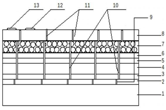
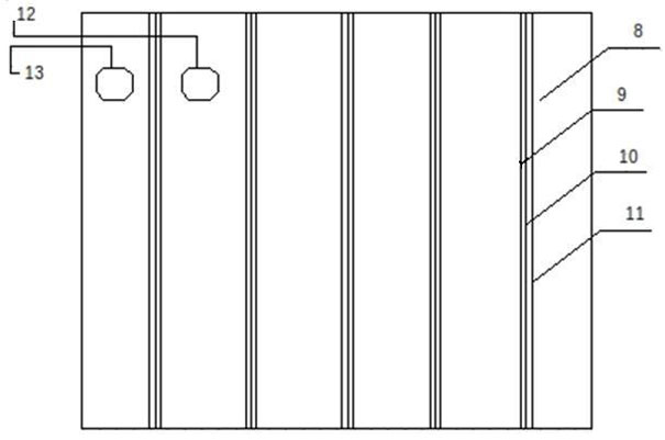
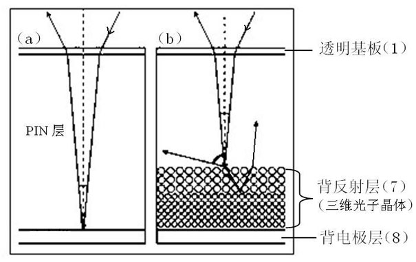
[0020] Specific Embodiment 1: In this embodiment, the three-dimensional photonic crystal is an amorphous silicon solar cell with a back reflection layer, including a front electrode layer 2, a P-SiC thin film layer 3, and an I-a-Si:H thin film layer stacked sequentially on a transparent substrate 1 4. N-a-Si:H film layer 5, back reflection layer 7, back electrode layer 8, first laser scribe line 9, second laser scribe line 10, mask wire 11, cathode wiring 12 and anode wiring 13, The amorphous silicon solar cell in which the three-dimensional photonic crystal is the back reflection layer also includes an ITO transparent conductive film 6, the back reflection layer 7 is a three-dimensional large-pore ordered aluminum-doped zinc oxide (AZO) film photonic crystal, and the ITO transparent conductive film 6 is located Between the back reflection layer 7 and the n-a-Si:H film layer 5.
[0021]In this embodiment, the amorphous silicon solar cells whose three-dimensional photonic cryst...
specific Embodiment approach 2
[0026] Embodiment 2: This embodiment differs from Embodiment 1 in that the thickness of the aluminum-doped zinc oxide thin film of the back reflection layer 7 is 0.5-1.5 μm, and the sheet resistance is 20-25 ohms / square. Other parameters are the same as in the first embodiment.
[0027] The back reflection layer of this embodiment is a three-dimensional photonic crystal, which can achieve omni-directional total reflection, and control the square resistance to 20-25 ohms / square, so as to achieve the purpose of reducing the series resistance as much as possible.
specific Embodiment approach 3
[0028] Embodiment 3: This embodiment differs from Embodiment 1 or Embodiment 2 in that the sheet resistance of the ITO transparent conductive film 6 is 5-10 ohms / square. Other parameters are the same as those in Embodiment 1 or Embodiment 2.
[0029] In this embodiment, the thickness of the ITO transparent conductive film 6 is 10-1000 nm, and the transmittance is greater than 80% in the wavelength range of 600 nm, which has no influence on the wavelength absorption and reflection of the solar cell.
PUM
| Property | Measurement | Unit |
|---|---|---|
| thickness | aaaaa | aaaaa |
| thickness | aaaaa | aaaaa |
| width | aaaaa | aaaaa |
Abstract
Description
Claims
Application Information
 - R&D Engineer
- R&D Manager
- IP Professional
- Industry Leading Data Capabilities
- Powerful AI technology
- Patent DNA Extraction
Browse by: Latest US Patents, China's latest patents, Technical Efficacy Thesaurus, Application Domain, Technology Topic, Popular Technical Reports.
© 2024 PatSnap. All rights reserved.Legal|Privacy policy|Modern Slavery Act Transparency Statement|Sitemap|About US| Contact US: help@patsnap.com


