
Method for actively packaging blue light LED chip based white light LED

A technology of LED chips and packaging methods, which is applied in the direction of electrical components, circuits, semiconductor devices, etc., can solve the problems of multiple processes, low production efficiency, and high cost, and achieve the effects of high process repeatability, high packaging efficiency, and short production time

Inactive Publication Date: 2009-11-04
SUN YAT SEN UNIV
View PDF2 Cites 6 Cited by
  • Summary
  • Abstract
  • Description
  • Claims
  • Application Information

AI Technical Summary

Problems solved by technology

The white light produced by this method has good color rendering, but the effective conversion efficiency is low. At the same time, the shift of the blue light emission wavelength, the change of intensity and the change of phosphor coating thickness will affect the uniformity of white light.
2) Utilize ultraviolet light or purple light LED+RGB phosphor powder; the conversion coefficient of purple light LED in this method can reach 0.8, the quantum conversion efficiency of each color phosphor powder can reach 0.9, and the color rendering of the obtained white light is better, but the same production method (1 ) similar problems, in addition, the fluorescent powder used in this system has poor luminescence stability and large light attenuation
[0006] There are many patents in the world for the packaging of white light diodes, but they are basically similar to the current LED packaging processes, mainly including dispensing, potting, and molding. The traditional packaging uses epoxy resin such as AB glue. Encapsulation by heat curing requires a long time (> 1 hour) to cure and post-cure the epoxy resin at a temperature higher than 100 degrees. There are many processes, low production efficiency, long cycle time, and high cost.
Specifically, it includes the following disadvantages: 1) The difficulty of process control is air bubbles, lack of material, and black spots; 2) In actual production, manual dispensing is often used, and the efficiency is low; 3) It needs molds to form, and most of them need lenses. In line with optical design; 4) Large-scale industrial production requires high equipment, and it is difficult for general enterprises to have enough funds to buy good equipment; 5) Thermal curing itself may affect the chip, causing the chip to be damaged due to high temperature
[0007] At present, some researchers use photosensitive resin to encapsulate light-emitting diodes to improve packaging efficiency, such as US patent 6958250 (applied in 2005), but the packaging process in this patent is similar to the current LED packaging process, which requires the use of molds
Chinese patent 200710032491.8 provides a light-curing packaging method that does not require a mold, but the shape of the lens formed by this method is not ideal, the mushroom-shaped structure is easy to fall off due to force, and is sensitive to the intensity and time of the incoming current, which is not suitable for automation. Production

Method used

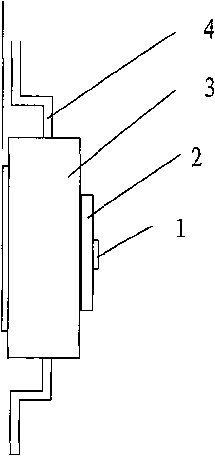
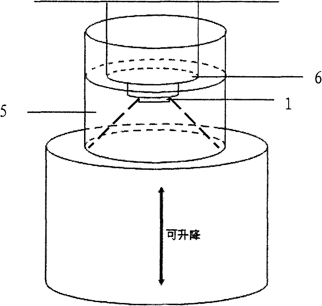

Image

  • Method for actively packaging blue light LED chip based white light LED
  • Method for actively packaging blue light LED chip based white light LED
  • Method for actively packaging blue light LED chip based white light LED

Examples


Embodiment

[0049] Example product test report

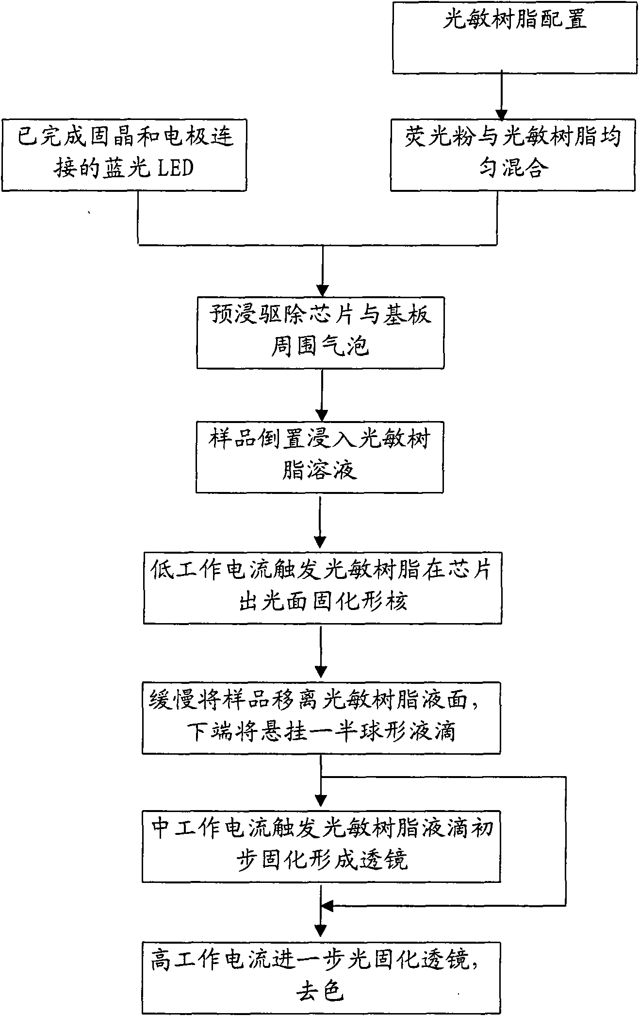
[0050] An advantage of the method of the present invention for packaging white light LEDs is that the light emitted by the LED chip itself is used to trigger the curing of the photosensitive resin, and the fluorescent powder is distributed in the resin lens as required, which can effectively solve the disadvantages of uneven fluorescent powder. After the sample is packaged, its light emission angle is greatly increased, close to 165°, while the prior art method of adding hemispherical lens molding and packaging can only reach 120°, its spatial distribution is more even, and the light emission effect is better. The test results of light and color parameters (without heat sink) show that the light radiation power, luminous flux, and luminous efficacy of this sample have met the commercial requirements of similar products, of which the luminous flux is 41.81m, and the luminous efficacy is 41.21m / W. The color rendering is higher than that of ge...


PUM


Abstract

The invention discloses a method for actively packaging a blue light LED chip based on white light LED, which comprises the following steps: preparing blue light-sensitive photosensitive resin liquid; mixing fluorescent powder into photosensitive resin; presoaking an LED semi-finished product in the photosensitive resin; inversely soaking the LED semi-finished product into the photosensitive resin liquid; soaking the edge of a chip substrate into the photosensitive resin; conducting low operating current to an LED chip to make the chip luminate; triggering the photosensitive resin to polymerize and forming a photosensitive resin core on light emergent surface of the LED chip; slowly lifting the LED semi-finished product to a liquid surface separating from the photosensitive resin liquid, wherein a semi-sphere or a semi-sphere like photosensitive resin liquid drop is attached to the photosensitive resin core and the chip substrate; conducting middle operating current for the LED chip to make the chip luminate, exciting the photosensitive resin liquid drop to solidify; conducting high operating current to a solidified sample of the photosensitive resin liquid drop to make the LED chip laminate; solidifying and decoloring the sample or decoloring the sample through insolation by the sun, or decolcoring by violetray irradiation; and finally cleaning the sample.

Description

technical field [0001] The invention belongs to the technical field of packaging of light-emitting diodes, in particular to an active packaging method for white LEDs based on blue LED chips. Background technique [0002] People have paid attention to the research on light-emitting diodes (LEDs), a light-emitting device that converts electrical energy into light energy. In 1993, high-brightness red and yellow LEDs began to appear. In 1995, high-brightness blue and green light-emitting diodes were successively developed. In addition to the performance, advantages and uses of ordinary LEDs, the wide-bandgap GaN-based blue and green LEDs have It also fundamentally solves the problem of lack of color in the three primary colors of LEDs, and is an indispensable key device for full-color display. On the other hand, the appearance of GaN-LED makes semiconductor white light solid-state lighting possible (referred to as "green lighting source"), bringing a revolution in lighting tech...

Claims


Application Information

Patent Timeline
Patent Type & Authority Applications(China)
IPC IPC(8): H01L33/00
Inventor 刘立林王钢蔡苗苗
Owner SUN YAT SEN UNIV
Learn More