Thermo-optical infrared detector and preparation method thereof
An infrared detector and manufacturing method technology, applied in chemical instruments and methods, optical radiation measurement, radiation pyrometry and other directions, can solve the problems of no design of infrared absorption layer, no vacuum packaging of devices, low noise equivalent temperature difference, etc. , to achieve the effect of easy batch production, low production difficulty, and improved filling factor
- Summary
- Abstract
- Description
- Claims
- Application Information
AI Technical Summary
Problems solved by technology
Method used
Image
Examples
Embodiment 1
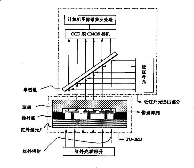
[0042] As shown in Figure 2, the provided TO-IRD consists of a silicon substrate 1, a pixel array 2, and a glass 3; the silicon substrate 1 not only acts as a substrate and a heat sink, but also acts as an infrared filter, while No special infrared filter is needed; the pixel array 2 is fabricated on the silicon substrate 1 , and the glass 3 and the silicon substrate 1 are connected by bonding to realize vacuum packaging of the pixel array 2 .
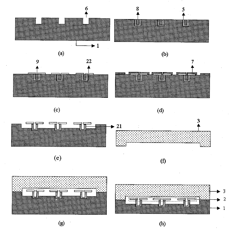
[0043] Combine below Figure 5 The process flow of this embodiment is described in detail, and the present invention is further described.
[0044] (1) Using photoresist or silicon oxide as a mask, etch the silicon substrate 1 by deep reactive ion etching (DRIE) or other methods to form a deep groove 6, the depth of the deep groove 6 is greater than 10 μm, and remove the mask layer, Such as Figure 5 as shown in a;
[0045] (2) The method of thermal oxidation or thermal oxidation, polysilicon growth, and secondary thermal ...
Embodiment 2
[0053] As shown in Figure 3, the provided TO-IRD consists of a silicon substrate 1, a pixel array 2, a glass 3 and an infrared filter 4; the silicon substrate 1 acts as a substrate and a heat sink; the pixel array 2 is fabricated on the silicon substrate 1, and the glass 3 is connected to the silicon substrate 1 by bonding, which improves the mechanical strength of the device, and the vacuum packaging of the pixel array 2 is realized by bonding the infrared filter 4 under the silicon substrate 1 .
[0054] Combine below Figure 6 The process flow of this embodiment is described in detail, and the present invention is further described.
[0055] (1) repeat the technological process of embodiment 1 (as Figure 5 shown in a-h), the process results are as follows Figure 6 as shown in a;
[0056] (2) Etch the silicon substrate 1 by deep reactive ion etching (DRIE) or other methods, and remove the silicon substrate below the pixel (except for the thermal insulation co...
Embodiment 3
[0059] As shown in Figure 2(b), the provided TO-IRD consists of a silicon substrate 1, a pixel array 2, and a glass 3; the silicon substrate 1 not only acts as a substrate and a heat sink, but also acts as an infrared filter. function without special infrared filter; the pixel array 2 is fabricated on the silicon substrate 1, and the glass 3 and the silicon substrate 1 are connected by bonding to realize the vacuum packaging of the pixel array 2. The difference from Embodiment 1 is that in order to further improve the heat insulation performance of the pixel, the heat insulation column in this embodiment is hollow.
[0060] Combine below Figure 7 The process flow of this embodiment is described in detail, and the present invention is further described.
[0061] (1) Using photoresist or silicon oxide as a mask, etch the silicon substrate 1 by deep reactive ion etching (DRIE) or other methods to form a deep groove 6, the depth of the deep groove 6 is greater than 10 μm,...
PUM
| Property | Measurement | Unit |
|---|---|---|
| thickness | aaaaa | aaaaa |
| height | aaaaa | aaaaa |
Abstract
Description
Claims
Application Information
 - R&D Engineer
- R&D Manager
- IP Professional
- Industry Leading Data Capabilities
- Powerful AI technology
- Patent DNA Extraction
Browse by: Latest US Patents, China's latest patents, Technical Efficacy Thesaurus, Application Domain, Technology Topic, Popular Technical Reports.
© 2024 PatSnap. All rights reserved.Legal|Privacy policy|Modern Slavery Act Transparency Statement|Sitemap|About US| Contact US: help@patsnap.com


