
InP base plane type back incident avalanche optoelectronic diode and manufacturing method thereof

A technology of avalanche optoelectronics and manufacturing methods, which is applied to circuits, electrical components, semiconductor devices, etc., and can solve problems such as good uniformity, difficult manufacturing, and difficult realization

Inactive Publication Date: 2009-10-07
INST OF SEMICONDUCTORS - CHINESE ACAD OF SCI
View PDF0 Cites 16 Cited by
  • Summary
  • Abstract
  • Description
  • Claims
  • Application Information

AI Technical Summary

Problems solved by technology

However, it is more difficult to achieve this for the thermal diffusion process, so it is not easy to manufacture planar avalanche photodiodes with good uniformity through the thermal diffusion-based process flow
In addition, suppressing the edge breakdown phenomenon of planar avalanche photodiodes is a very important issue, although measures such as guard rings are adopted in the traditional method, the edge breakdown phenomenon still exists to a large extent

Method used


Image

  • InP base plane type back incident avalanche optoelectronic diode and manufacturing method thereof
  • InP base plane type back incident avalanche optoelectronic diode and manufacturing method thereof
  • InP base plane type back incident avalanche optoelectronic diode and manufacturing method thereof

Examples


Embodiment Construction

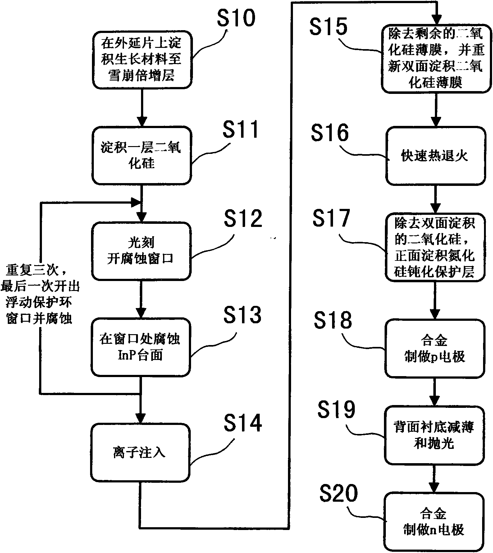
[0040] see figure 1 Shown, a kind of InP base planar type back-incidence avalanche photodiode of the present invention comprises:

[0041] a substrate 10;

[0042] A buffer layer 20, the buffer layer 20 is fabricated on the substrate 10;

[0043] An absorption layer 30, the absorption layer 30 is made on the buffer layer 20, and the absorption layer 30 is InGaAs;

[0044] A transition layer 40, the transition layer 40 is made on the absorption layer 30, and the transition layer 40 is InGaAsP;

[0045] An electric field control layer 50, the electric field control layer 50 is fabricated on the transition layer 40;

[0046] An avalanche multiplication layer 60, the avalanche multiplication layer 60 is fabricated on the electric field control layer 50;

[0047] Wherein the central region above the avalanche multiplication layer 60 is formed with a recessed portion 61, the edge of the recessed portion 61 is an inverted stepped structure; the outer side of the upper recessed po...


PUM


Abstract

The invention relates to an InP base plane type back incident avalanche optoelectronic diode which comprises a substrate, a buffer layer manufactured on the substrate, an absorption layer manufactured on the buffer layer, a transition layer manufactured on the absorption layer, an electric field control layer manufactured on the transition layer and an avalanche multiplication layer manufactured on the electric field control layer, wherein a concave part is disposed on a central area on the avalanche multiplication layer, and the edge of the concave part is of an inverse step-shaped structure; a floating protective ring is manufactured at the outside of the concave part on the avalanche multiplication layer; the concave part comprises a P-type doped layer disposed on the bottom surface of the concave part and a passivation protecting layer disposed on the surfaces of the P-type doped layer and the avalanche multiplication layer, wherein a contact through hole is disposed in the center of the passivation protecting layer, and a P electrode is manufactured at the bottom in the middle of the passivation protecting layer; and an n electrode is manufactured on the back of the substrate, and a light incident window is disposed in the middle of the n electrode.

Description

technical field [0001] The invention relates to a semiconductor device, in particular to an InP-based planar back-incidence avalanche photodiode and a manufacturing method thereof. Background technique [0002] As an important photodetector element, avalanche photodiodes have been widely used in communication, radar, biomolecular luminescence detection and single photon detection in the laboratory. From the perspective of device structure and manufacturing process, avalanche photodiodes can be divided into mesa structure and planar structure. For the avalanche photodiode with mesa structure, each doped layer is generated by deposition, and all parts in the passivation layer are active regions; for the avalanche photodiode with planar structure, the doping of the front active region is Formed by thermal diffusion or ion implantation, there is a large undoped intrinsic region around the active region. Since the avalanche photodiode with the mesa structure has the insurmounta...

Claims


Application Information

Patent Timeline
Patent Type & Authority Applications(China)
IPC IPC(8): H01L31/107H01L31/18
Inventor 吴孟陈燕凌杨富华曹延名
Owner INST OF SEMICONDUCTORS - CHINESE ACAD OF SCI
Learn More