
InAlAs avalanche photodetector and production method thereof

An avalanche photoelectric and detector technology, used in circuits, electrical components, semiconductor devices, etc., can solve problems such as edge breakdown, and achieve the effects of suppressing edge breakdown, simplifying fabrication processes, and avoiding guard ring structures.

Pending Publication Date: 2021-01-29
THE 13TH RES INST OF CHINA ELECTRONICS TECH GRP CORP
View PDF6 Cites 3 Cited by
  • Summary
  • Abstract
  • Description
  • Claims
  • Application Information

AI Technical Summary

Problems solved by technology

[0005] In view of this, the embodiment of the present invention provides an InAlAs avalanche photodetector and its preparation method to solve the problem of edge breakdown of the electron injection avalanche photodetector in the prior art

Method used


Image

  • InAlAs avalanche photodetector and production method thereof
  • InAlAs avalanche photodetector and production method thereof
  • InAlAs avalanche photodetector and production method thereof

Examples


Embodiment Construction

[0050] In the following description, specific details such as specific system structures and technologies are presented for the purpose of illustration rather than limitation, so as to thoroughly understand the embodiments of the present invention. It will be apparent, however, to one skilled in the art that the invention may be practiced in other embodiments without these specific details. In other instances, detailed descriptions of well-known systems, devices, circuits, and methods are omitted so as not to obscure the description of the present invention with unnecessary detail.

[0051] In order to illustrate the technical solutions of the present invention, specific examples are used below to illustrate.

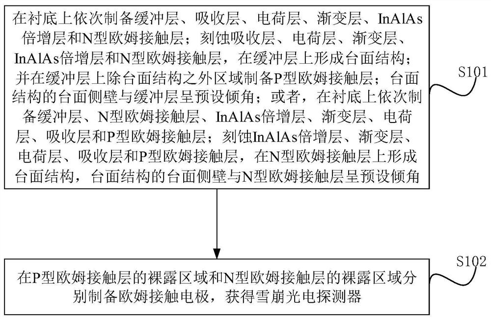
[0052] figure 1 The implementation flow diagram of the manufacturing method of the InAlAs avalanche photodetector provided by the embodiment of the present invention is described in detail as follows.

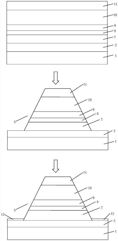
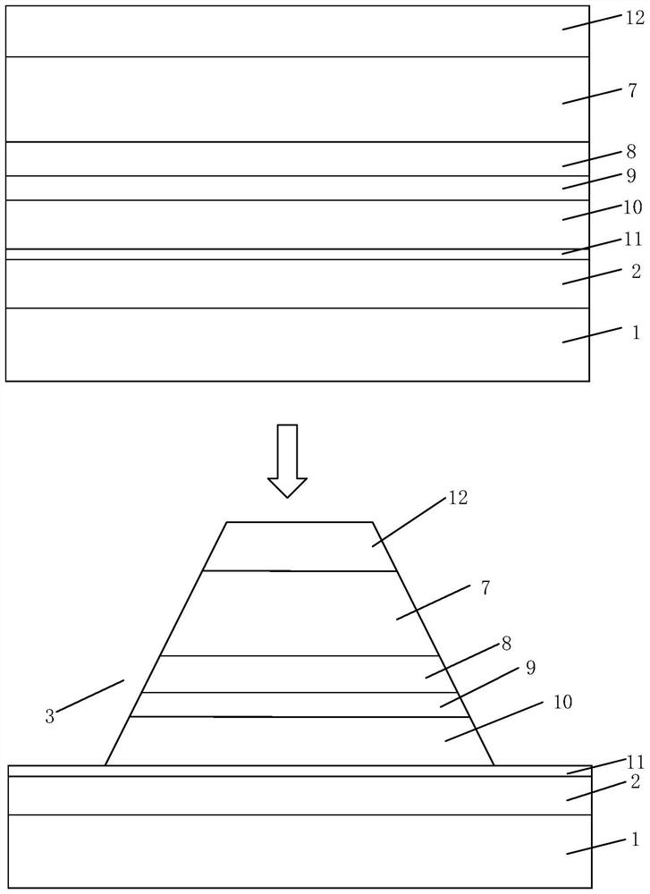
[0053] Step S101, see figure 2 and image 3 Prepare buffer lay...


PUM

PropertyMeasurementUnit
angleaaaaaaaaaa
thicknessaaaaaaaaaa
thicknessaaaaaaaaaa

Abstract

The invention is applicable to the technical field of photodetectors, and provides an InAlAs avalanche photodetector and a production method thereof. The method comprises the steps of sequentially preparing a buffer layer, an absorption layer, a charge layer, a gradient layer, an InAlAs multiplication layer and an N-type ohmic contact layer on a substrate and etching to form a mesa structure witha mesa side wall forming a preset inclination angle with the buffer layer, and preparing a P-type ohmic contact layer on the buffer layer except for the mesa structure; or preparing the buffer layer,the N-type ohmic contact layer, the InAlAs multiplication layer, the gradient layer, the charge layer, the absorption layer and the P-type ohmic contact layer on the substrate in sequence and etchingto form the mesa structure with a preset inclination angle between the mesa side wall and the N-type ohmic contact layer; and preparing ohmic contact electrodes in an exposed area of the P-type ohmiccontact layer and the exposed area of the N-type ohmic contact layer respectively, and acquiring the InAlAs avalanche photodetector. Edge breakdown can be suppressed through the mesa structure with the preset inclination angle, and the process is simple.

Description

technical field [0001] The invention belongs to the technical field of photodetectors, and in particular relates to an InAlAs avalanche photodetector and a preparation method thereof. Background technique [0002] Photodetectors are devices that convert optical signals into electrical signals. As the core part of optical receivers, the performance of photodetectors determines the transmission capacity of optical fiber communication systems. With the development of optical fiber communication technology, the performance requirements of photodetectors are getting higher and higher. Compared with the traditional PIN structure detector, the avalanche multiplication effect generated by the carriers inside the avalanche photodetector under the bias voltage can greatly improve the sensitivity of photoelectric signal detection, thereby improving the response of the device and the signal-to-noise ratio, etc. . Therefore, in optical fiber communication systems, avalanche photodetect...

Claims


Application Information

Patent Timeline
Patent Type & Authority Applications(China)
IPC IPC(8): H01L31/18H01L31/0304H01L31/0352H01L31/107
CPCH01L31/107H01L31/03046H01L31/1844H01L31/03529Y02P70/50
Inventor 韩孟序尹顺政齐利芳
Owner THE 13TH RES INST OF CHINA ELECTRONICS TECH GRP CORP
Learn More