


Quick Research
Generate reliable direction feasibility study reports for your R&D in just a few steps.

Technical Q&A
Discover and master advanced knowledge NOW. Basics, ideas, possibilities, all at once.

Find Solutions
As an expert in R&D theories, this can generate solutions to your technical problems instantly.

Evaluate Feasibility
Analyze your overall solution with one click, know your potential R&D risks in advance.

Monitor Landscape
Get weekly tech updates, stay abreast of the latest tech innovations and key insights.
Preparation of inorganic silicon dioxide nano template
A silicon dioxide and nanotechnology, applied in the field of nano-template preparation, can solve the problems of low surface energy of PDMS and the influence of micro-region structure regularity, etc., and achieve the effect of avoiding the difficulty of peeling, eliminating the need for processing procedures, and good thermal stability
- Summary
- Abstract
- Description
- Claims
- Application Information
AI Technical Summary
Problems solved by technology
Method used
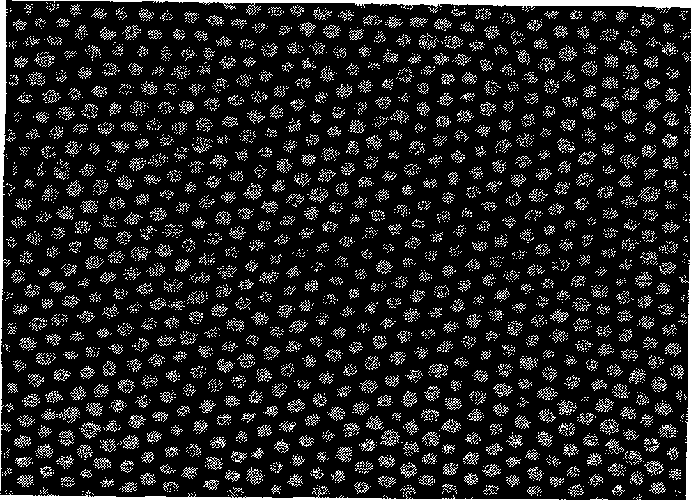
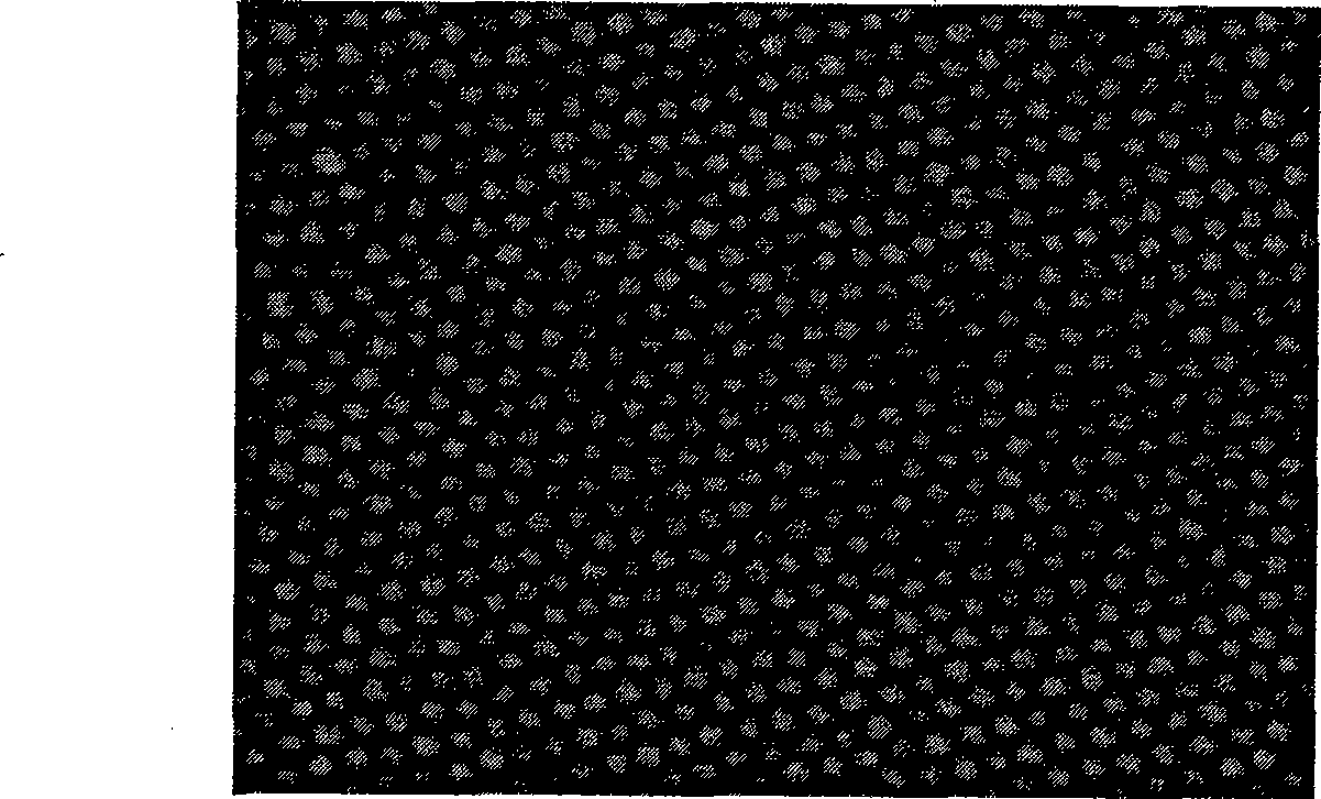
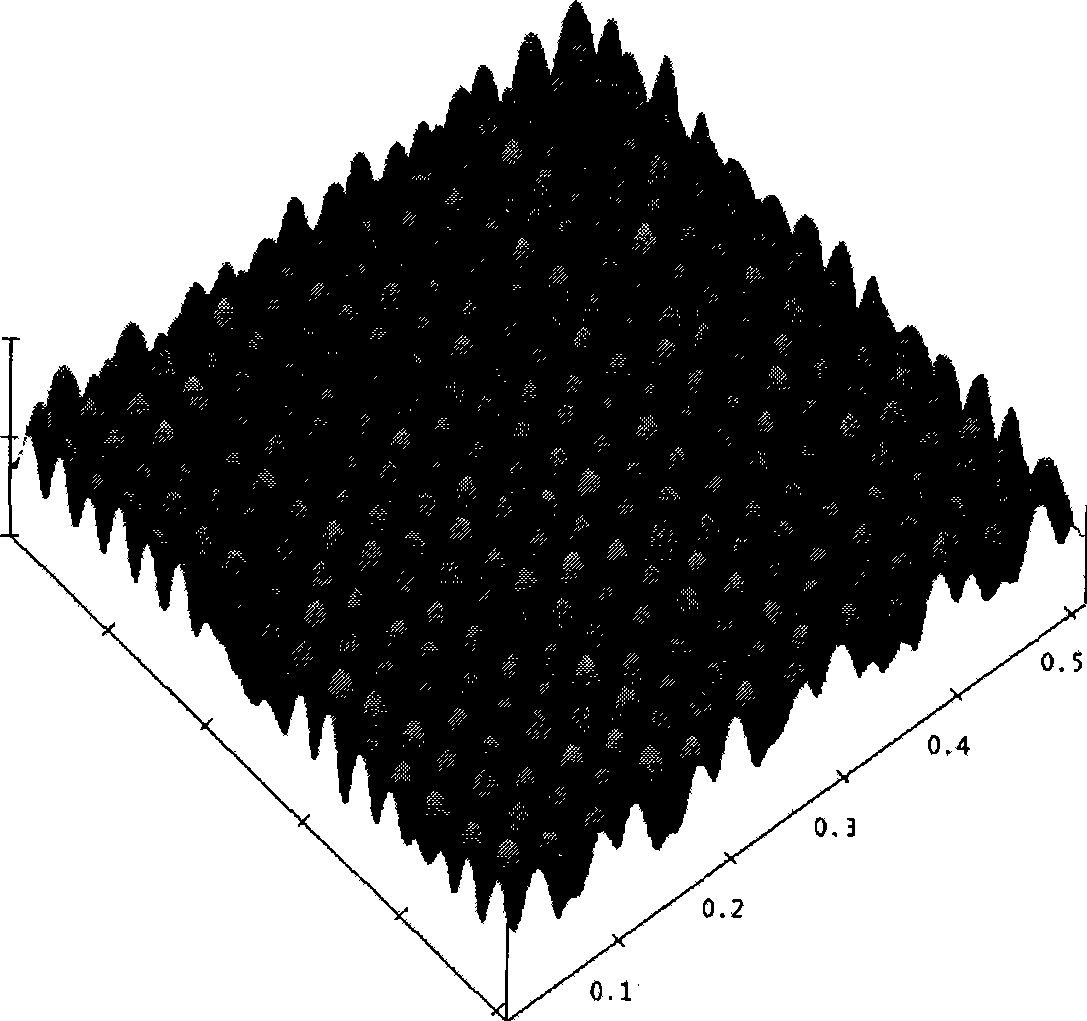
Image

Examples
Embodiment 1
[0034] The PS-PDMS block copolymer (the number-average molecular weight is 15000, PDMS weight fraction 10%) that is dissolved in toluene and is 0.2% by weight percent concentration, obtains the macromolecular solution of homogeneous dispersion with ultrasonic treatment at room temperature for 0.5 hour; After the solution is filtered, the block copolymer solution is spin-coated on the silicon wafer substrate at a rotation speed of 1000 rpm by spin coating method at room temperature, and the residual solvent in the film is vaporized at room temperature to obtain a film with a thickness of 20 nm. ; The film was heat-treated at 140 °C for 12 hours in a nitrogen atmosphere to cause microphase separation of PS and PDMS; finally, UV-O 3 (The wavelength of ultraviolet light is 185 nanometers and 254 nanometers) under the synergistic effect for 5 minutes, the PS phase is etched, and the regularly arranged PDMS phase is oxidized to inorganic SiO 2 Mutually.
Embodiment 2
[0036] The PMMA-PDMS block copolymer (the number-average molecular weight is 20000, PDMS weight fraction 15%) that is dissolved in toluene and is 0.5% by weight percent concentration, obtains the macromolecule solution of homogeneous dispersion with ultrasonic treatment 1 hour at normal temperature; After the solution is filtered, the block copolymer solution is spin-coated on a silicon wafer substrate at a rotation speed of 1000 rpm by spin coating method at room temperature, and the residual solvent in the film is vaporized at room temperature to obtain a film with a thickness of 35 nm. ; The film was heat-treated at 170 ° C for 18 hours in a nitrogen atmosphere to cause microphase separation of PMMA and PDMS; finally, the oxygen plasma was treated for 20 seconds to etch the PMMA phase, and at the same time the regularly arranged PDMS phase was oxidized to inorganic SiO 2 Mutually.
Embodiment 3
[0038] The PS-PDMS block copolymer (the number-average molecular weight is 35000, PDMS weight fraction 19%) that is dissolved in toluene and the weight percent concentration is 1%, obtains the macromolecular solution of homogeneous dispersion with ultrasonic treatment at room temperature for 1.5 hours; After the solution is filtered, the block copolymer solution is spin-coated on the silicon wafer substrate at a rotation speed of 5000 rpm by spin coating method at room temperature, and the residual solvent in the film is vaporized at room temperature to obtain a film with a thickness of 25 nm. ; The film was heat-treated at 200 °C for 24 hours in a nitrogen atmosphere to cause microphase separation of PS and PDMS; finally, UV-O 3 (The wavelength of ultraviolet light is 185 nanometers and 254 nanometers) under the synergistic effect for 10 minutes, the PS phase is etched, and the regularly arranged PDMS phase is oxidized to inorganic SiO 2 Mutually. The resulting inorganic sil...
PUM
| Property | Measurement | Unit |
|---|---|---|
| thickness | aaaaa | aaaaa |
| molecular weight distribution | aaaaa | aaaaa |
Abstract
Description
Claims
Application Information
 - R&D Engineer
- R&D Manager
- IP Professional
- Industry Leading Data Capabilities
- Powerful AI technology
- Patent DNA Extraction
Browse by: Latest US Patents, China's latest patents, Technical Efficacy Thesaurus, Application Domain, Technology Topic, Popular Technical Reports.
© 2024 PatSnap. All rights reserved.Legal|Privacy policy|Modern Slavery Act Transparency Statement|Sitemap|About US| Contact US: help@patsnap.com