
Method for manufacturing contact window for reducing contact resistance

A manufacturing method and contact resistance technology, applied in semiconductor/solid-state device manufacturing, circuits, electrical components, etc., can solve problems affecting process reliability and component performance, eroding borophosphosilicate glass layers, etc., to prevent expansion and avoid excessive The effect of erosion

Inactive Publication Date: 2009-04-01
POWERCHIP SEMICON CORP
View PDF0 Cites 3 Cited by
  • Summary
  • Abstract
  • Description
  • Claims
  • Application Information

AI Technical Summary

Problems solved by technology

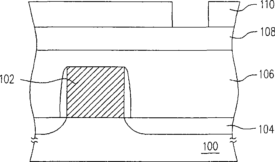
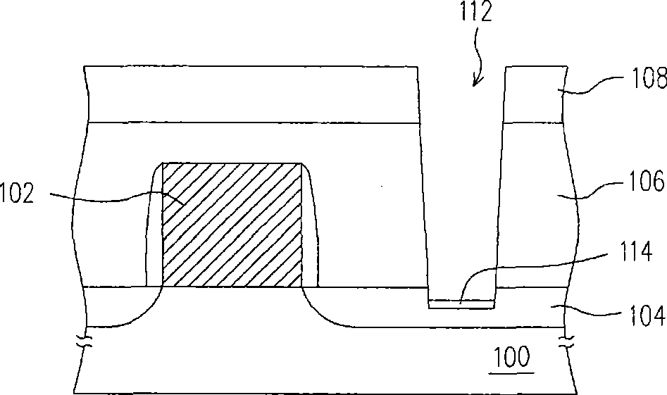
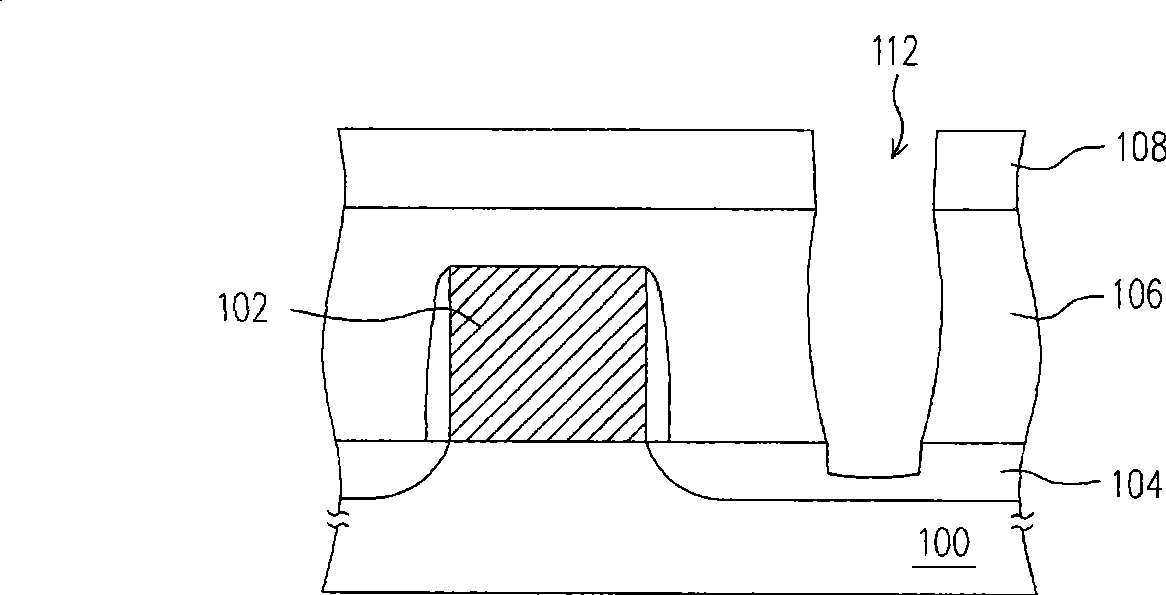
However, while removing the native oxide layer 114, part of the borophosphosilicate glass layer 106, the silicon oxide layer 108 and the silicon substrate 100 will also be corroded.
In particular, the doped borophosphosilicate glass layer 106 has greater wet etching selectivity than the undoped silicon oxide layer 108, so that the sidewall of the opening 112 will be over-eroded and concave, resulting in The critical dimension (CD) of the subsequent preformed contact window is too large
In addition, if the silicon substrate 100 at the bottom of the opening 112 is corroded by the etchant and dented, it will seriously affect the reliability of the process and the performance of the device.

Method used


Image

  • Method for manufacturing contact window for reducing contact resistance
  • Method for manufacturing contact window for reducing contact resistance
  • Method for manufacturing contact window for reducing contact resistance

Examples


Embodiment Construction

[0061] Figure 2A to Figure 2C is a schematic cross-sectional view of the manufacturing process of the contact window according to an embodiment of the present invention.

[0062] Please refer to Figure 2A , providing a substrate 200, which is, for example, a silicon substrate. A gate structure 220 has been formed on the substrate 200 . The gate structure 220 may be a gate structure in a dynamic random access memory (DRAM), a gate structure in a metal oxide semiconductor (MOS), or a gate structure in other semiconductor devices, The present invention is not particularly limited. In this embodiment, the gate structure 220 is composed of, for example, a floating gate 220a, a control gate 220b, an inter-gate dielectric layer 220c, a tunnel dielectric layer 220d, and a top cap layer 220e. The material of the floating gate 220 a and the control gate 220 b is, for example, a doped polysilicon layer, and the formation method thereof is, for example, chemical vapor deposition. T...


PUM


Abstract

The invention provides a preparation method for a contact window that reduces contact resistance. Firstly, a substrate, on which a protective layer and a dielectric layer are successively formed, is provided. Afterward, a dry etching process is carried out so as to remove a part of the dielectric layer, thus forming an opening which exposes a part of the protective layer. Then, a wet cleaning process is performed. After that, a dry cleaning process is performed so as to remove the protective layer positioned at the bottom of the opening, and a conductor layer is formed in the opening afterward.

Description

technical field [0001] The invention relates to a semiconductor process, in particular to a method for manufacturing a contact window capable of reducing contact resistance. Background technique [0002] With the rapid development of semiconductor process technology, in order to increase the speed and performance of components, the size of the entire circuit components must be continuously reduced, and the integration of components must be continuously improved. In the case of requiring higher and higher integration of components, changes in the physical characteristics of the components (such as contact resistance between components) must also be considered to avoid affecting the operating speed and performance of the components. [0003] Taking memory as an example, a memory cell is usually composed of a transistor and a capacitor. A transistor includes a gate and source / drain regions. The gate of the transistor is electrically connected to a corresponding word line (WL)...

Claims


Application Information

Patent Timeline
Patent Type & Authority Applications(China)
IPC IPC(8): H01L21/768
Inventor 陈正坤简俊弘吴至宁廖玉梅王伟民陈泳卿谢荣源吴欣雄
Owner POWERCHIP SEMICON CORP
Learn More