
Aurum-nickel doped monocrystalline silicon sheet type negative temperature coefficient heat-variable resistor and method for making same

A negative temperature coefficient, single crystal silicon wafer technology, applied in the direction of resistors with negative temperature coefficient, resistance manufacturing, resistors, etc., can solve the problem of no technical report of single crystal silicon chip thermistor, and achieve low cost , the effect of simple process

Inactive Publication Date: 2011-03-23
XINJIANG TECHN INST OF PHYSICS & CHEM CHINESE ACAD OF SCI
View PDF0 Cites 0 Cited by
  • Summary
  • Abstract
  • Description
  • Claims
  • Application Information

AI Technical Summary

Problems solved by technology

[0006] At present, there is no relevant technical report on the development of monocrystalline silicon chip thermistors by using the method of high-temperature diffusion of gold and nickel impurities in single crystal silicon.

Method used


Image

  • Aurum-nickel doped monocrystalline silicon sheet type negative temperature coefficient heat-variable resistor and method for making same
  • Aurum-nickel doped monocrystalline silicon sheet type negative temperature coefficient heat-variable resistor and method for making same

Examples


Embodiment 1

[0025] Adopt n-type Czochralski single-crystal silicon wafer with a resistivity of 1Ω·cm, the crystal plane is (111) plane, the radial distribution of resistivity is ≤±5%. Ultrasonic desanding in deionized water for 5 minutes, ultrasonic degreasing in acetone for 5 minutes, use ammonia water, hydrogen peroxide and deionized water according to the ratio of 1:2:5 to boil for 15 minutes, and then use hot and cold deionization Wash with water for 3-5 times, and finally dehydrate with acetone for later use;

[0026] Place the cleaned silicon wafer flat on the filter paper and use NiCl 2 ·6H 2 The concentration of O is 2.1×10 -4 mol / ml solution and AuCl 3 ·HCl·4H 2 The concentration of O is 1.2×10 -4 The mol / ml solution is mixed at a ratio of 3:1 by volume and dropped on the surface of the silicon wafer, dried under an infrared lamp until the surface becomes a uniform white crystal, diffused at a high temperature in a constant temperature environment, and the diffusion temperat...


PUM

PropertyMeasurementUnit
electrical resistanceaaaaaaaaaa
electrical resistivityaaaaaaaaaa

Abstract

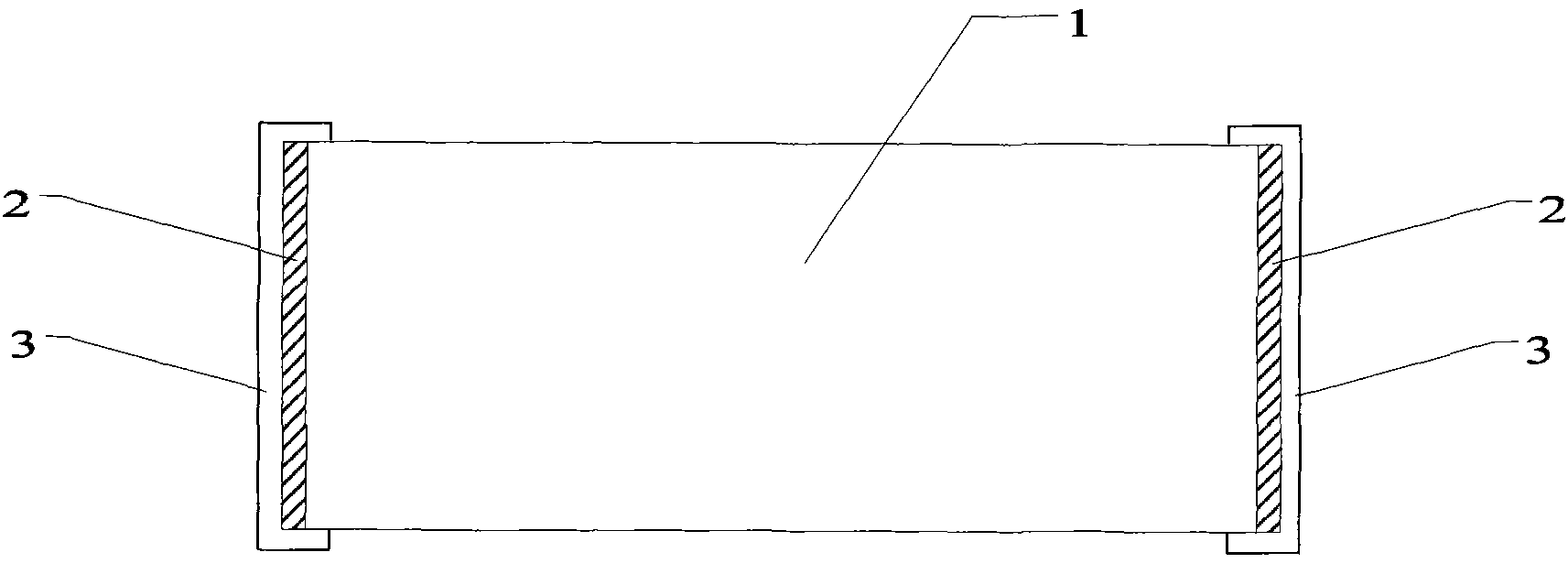
The invention relates to gold and nickel doped monocrystal line silicon wafer thermistor. The thermal resistor adopts a coating source high temperature diffusion method. Transition metals of gold and nickel are used as doping agents and are doped in n-type monocrystal line silicon. The electrical compensation performance of gold and nickel in the n-type monocrystal line silicon is used for preparing negative temperature coefficient thermal-sensitive material. The scribing is implemented on a precise scribing machine. Electrodes are prepared on two ends of a chip. Two-layer structure of nickeland silver is adopted by the electrodes. The ohmic contact between silicon crastal and the electrons is realized. The silicon thermal-sensitive functional material bases on a monocrystal line siliconsemiconductor and is doped with gold and nickel metal ions. A deep level capture center is formed. The material generates thermal characteristics. Through the strict control on the concentration and the distribution of the doped irons in silicon, high B value low resistance elements which are hard realized by oxide ceramic thermal-sensitive material can be realized easily. The consistency, the repeatability and the stability of the high thermal-sensitive material and the elements are improved.

Description

technical field [0001] The invention relates to a gold and nickel doped single crystal silicon chip type negative temperature coefficient thermistor and a preparation method thereof, belonging to the thermistor field of sensor technology in the information field. Background technique [0002] Due to the rapid development of surface mount technology (SMT). Component groups that were treated as special-shaped components in the past have gradually developed into surface mount components (SMD), and a new understanding of its technology has become an imminent task. Because the thermistor has the characteristics of high temperature measurement accuracy, good interchangeability, and high reliability, it is widely used in temperature measurement, control, and compensation. [0003] At present, thermistors have occupied more than 40% of the market share in the entire field of temperature-sensitive devices. With the increasing demand for high-precision thermal devices in intelligent ...

Claims


Application Information

Patent Timeline
Patent Type & Authority Patents(China)
IPC IPC(8): H01C7/04H01C17/00
Inventor 陈朝阳范艳伟董茂进丛秀云陶明德王军华
Owner XINJIANG TECHN INST OF PHYSICS & CHEM CHINESE ACAD OF SCI
Learn More