
Film resistor structure and method for manufacturing same

A technology of thin film resistors and manufacturing methods, which is applied in the direction of resistors, coated resistive materials, non-adjustable metal resistors, etc., can solve the problems that thin film resistor products have not been recognized by the market, cannot become market products, and have low resistance values

Active Publication Date: 2009-04-01
IND TECH RES INST +1
View PDF0 Cites 2 Cited by
  • Summary
  • Abstract
  • Description
  • Claims
  • Application Information

AI Technical Summary

Problems solved by technology

From the 1980s to the present, although thin-film resistor products had a good market acceptance in the early 1990s, they were limited by the immaturity of the overall embeddable component technology environment and the low resistance and cost. The shortcomings of high-level characteristics, coupled with the continued advancement of competing technologies - surface mount technology (SMT) - such as the launch of 0201 and competition from technologies such as organic polymer thick film resistors (PTF) with the same application alternatives, have so far thin film Resistor products have not been recognized by the market and cannot become the mainstream of market products
However, as far as the size limit of the next generation 01005 is concerned, whether it is a surface mount (SMT) process or a organic thick film (PTF) product, there are precision problems that are difficult to overcome, so it has once again aroused the market's interest in planar embeddable thin film resistors. expectations
But relatively, the shortcoming of the sheet resistance value of the thin film resistor product is too low must be overcome first

Method used

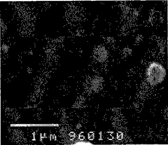
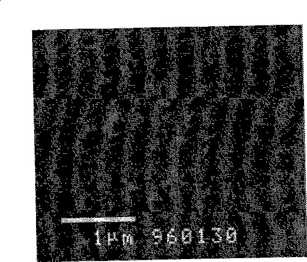

Image

  • Film resistor structure and method for manufacturing same
  • Film resistor structure and method for manufacturing same
  • Film resistor structure and method for manufacturing same

Examples


no. 1 example

[0025] In this embodiment, a semiconductor metal oxide layer (such as copper oxide or cuprous oxide) with a fixed content is formed on the substrate, and a conductive metal layer (such as palladium) with different numbers of layers is formed above it, and the content of the conductive metal is observed. The effect of the change. The following is a description of the process steps.

[0026] Taking two glass slides as substrates, five layers of cuprous oxide (Cu 2 O) production, its total thickness is about 0.1 μm. Afterwards, the group A test pieces were subjected to a transfer annealing treatment for about 60 minutes in a heating furnace at a temperature of about 350°C. After annealing, cuprous oxide is converted to copper oxide (CuO). The test pieces of group B have not been annealed, so they are still cuprous oxide (Cu 2 O).

[0027] Then, using chloroform solution as a carrier, palladium acetate (Pd(OAc) 2 ) was mixed in a chloroform solution (0.1g / 16cc) and applied. ...

no. 2 example

[0037] In this embodiment, a conductive metal layer (such as palladium) with a fixed content is first formed on the substrate, and then a semiconductor metal oxide layer (such as copper oxide) with different layers is formed on the substrate, and the content of the semiconductor metal oxide layer is observed. The effect of the change. The following is a description of the process steps.

[0038] Take three glass slides as the base material, carry out secondary palladium acetate (Pd(OAc) 2 ) Spin-Coating operation of chloroform solution (0.1g / 16cc). Among them, thermal decomposition at 200°C for about 15 minutes after the first spin-coating of palladium acetate, and thermal decomposition at 200°C for about 60 minutes after the second spin-coating of palladium acetate to reduce the palladium metal.

[0039] Then copper acetate (Cu(OAc) 2 ) alcohol solution (0.1g / 16cc) for 1, 3 and 4 times of spin-coating (Spin-Coating) operations, and after each coating operation is completed...


PUM


Abstract

The invention relates to a film resistor structure which at least comprises a substrate and a composite film resistor which is formed at the substrate. The composite film resistor is formed by mixing semiconductor metal copper or / and nickel oxide which is provided with negative temperature coefficient of resistance (TCR) and conductive metal material which is provided with positive temperature coefficient of resistance in dispersed way. Thus, when the resistance value of a film resistance chip is improved to be larger than 1000 Omega / square area, the value of TCR can still be guaranteed to be less than 200ppm / DEG C effectively.

Description

technical field [0001] The invention relates to a thin-film resistance structure and a manufacturing method thereof, in particular to a thin-film resistance structure with high sheet resistance and low temperature coefficient of resistance and a manufacturing method thereof. Background technique [0002] Copper foil lines and resistors are both necessary components on the printed circuit board (PCB). In current industrial applications, the application and processing of the two are separate and irrelevant. Among them, the copper foil circuit is firstly laminated with copper foil (copper-clad laminate, CCL), and then supplemented by developing / etching / stripping (DES) and other procedures to complete the production of the circuit. As for the installation and configuration of the resistor components, after purchasing separate resistor components, the individual resistor components are assembled using surface mount (SMT) technology. However, with the development trend of mobile ...

Claims


Application Information

Patent Timeline
Patent Type & Authority Applications(China)
IPC IPC(8): H01C7/00H01C17/06
Inventor 陈友忠李鸿坤翁荣洲
Owner IND TECH RES INST
Learn More