
Adamantane based molecular glass photoresists for sub-200 nm lithography

A photoresist, adamantane technology, applied in the field of amorphous glass photoresist, can solve the problems of increased use of short exposure wavelengths, poor resolution, etc.

Inactive Publication Date: 2009-03-18
CORNELL RES FOUNDATION INC +1
View PDF1 Cites 2 Cited by
  • Summary
  • Abstract
  • Description
  • Claims
  • Application Information

AI Technical Summary

Problems solved by technology

For example, current photoresists can be highly opaque to short exposure wavelengths such as 193nm, thereby resulting in poorer resolution imaging
[0007] Also, the increased use of such short exposure wavelengths is inevitable, as short wavelengths are required to form smaller features (<0.50 or <0.25)

Method used


Image

  • Adamantane based molecular glass photoresists for sub-200 nm lithography
  • Adamantane based molecular glass photoresists for sub-200 nm lithography
  • Adamantane based molecular glass photoresists for sub-200 nm lithography

Examples


Embodiment Construction

[0092] specific implementation plan

[0093] The present disclosure relates to low molecular weight photoresist materials that form stable glasses above room temperature. The disclosed photoresists offer several advantages over conventional linear polymers as pattern feature sizes are reduced. First, the disclosed materials are amorphous and have low molecular weight. Therefore, they do not suffer from chain entanglement. Since the disclosed materials have smaller molecular sizes and higher densities of sterically crowded peripheral molecules, the disclosed photoresists are expected to reduce line width roughness (LWR) at smaller design sizes. ) and changes in line edge roughness (LER).

[0094] In addition, the uniform small molecular size provides excellent processability, elasticity, transparency, and uniform solubility. Any photoresist material used for 193nm exposure or immersion 193nm exposure must have high plasma resistivity and superior optical properties as well ...


PUM

PropertyMeasurementUnit
wavelengthaaaaaaaaaa

Abstract

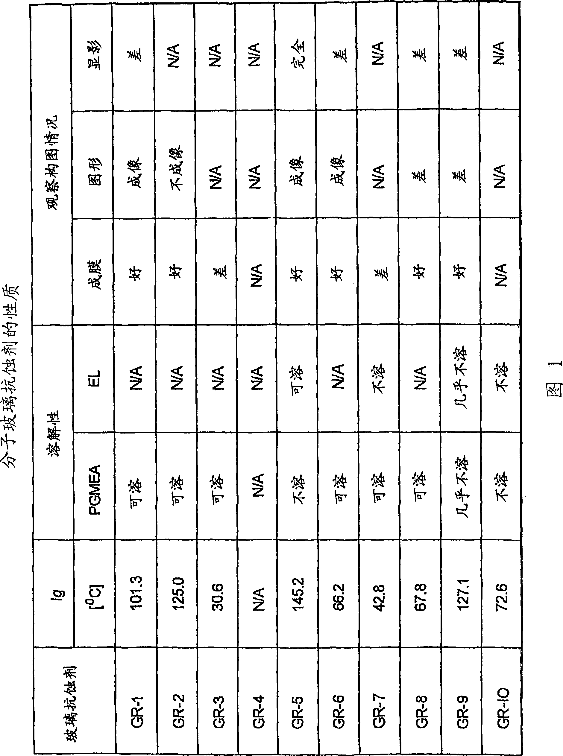
Disclosed are glass photoresists generated from adamantane derivatives containing acetal and / or ester moieties as novel high-performance photoresist materials. Some of the disclosed adamantane-based glass resists have a tripodal structure and other disclosed adamantane-based glass resists include one or more cholic groups. The disclosed adamantane derivatives can be synthesized from starting materials which are commercially available. By way of example only, one of many disclosed amorphous glass photoresists has the following structure: GR-5 Adamantane-l,3,5-triyltris(oxymethylene) tricholate.

Description

technical field [0001] The present invention discloses adamantane-based amorphous glass photoresists having acetal and / or ester moieties for exposure at wavelengths below 200 nm (sub-200 nm). The disclosed photoresist reduces line width roughness (LWR) and line edge roughness (LER) variation at smaller dimensions. Background technique [0002] To meet the demand for faster performance, integrated circuit devices continue to become smaller and smaller. The fabrication of integrated circuit devices with smaller features introduces new challenges in many of the fabrication methods routinely used in semiconductor fabrication. One fabrication method that is particularly affected is photolithography. [0003] In semiconductor lithography, a light-sensitive film in the form of a photoresist is used to transfer an image into a substrate. A photoresist coating is formed on the substrate, and the photoresist layer is then exposed to activating radiation through a photomask. The ph...

Claims


Application Information

Patent Timeline
Patent Type & Authority Applications(China)
IPC IPC(8): G03C1/73G03F7/20G03F7/30
CPCC07C2103/74C07C67/14C07C41/52G03F7/004C07C43/303C07H15/18C07C69/753C07C41/48C07C41/22G03F7/0392C07J9/005C07H9/04C07C2603/74C07C43/192C07C43/30
Inventor 田中真治克里斯托弗·K·奥伯
Owner CORNELL RES FOUNDATION INC
Learn More