
Photomask testing method, photomask manufacture method, electronic component manufacture method, testing mask and testing mask set

An inspection method and a technology for testing masks, which are applied in semiconductor/solid-state device testing/measurement, originals for opto-mechanical processing, electrical components, etc. Difficulty matching conditions

Inactive Publication Date: 2008-12-03
HOYA CORP
View PDF2 Cites 12 Cited by
  • Summary
  • Abstract
  • Description
  • Claims
  • Application Information

AI Technical Summary

Problems solved by technology

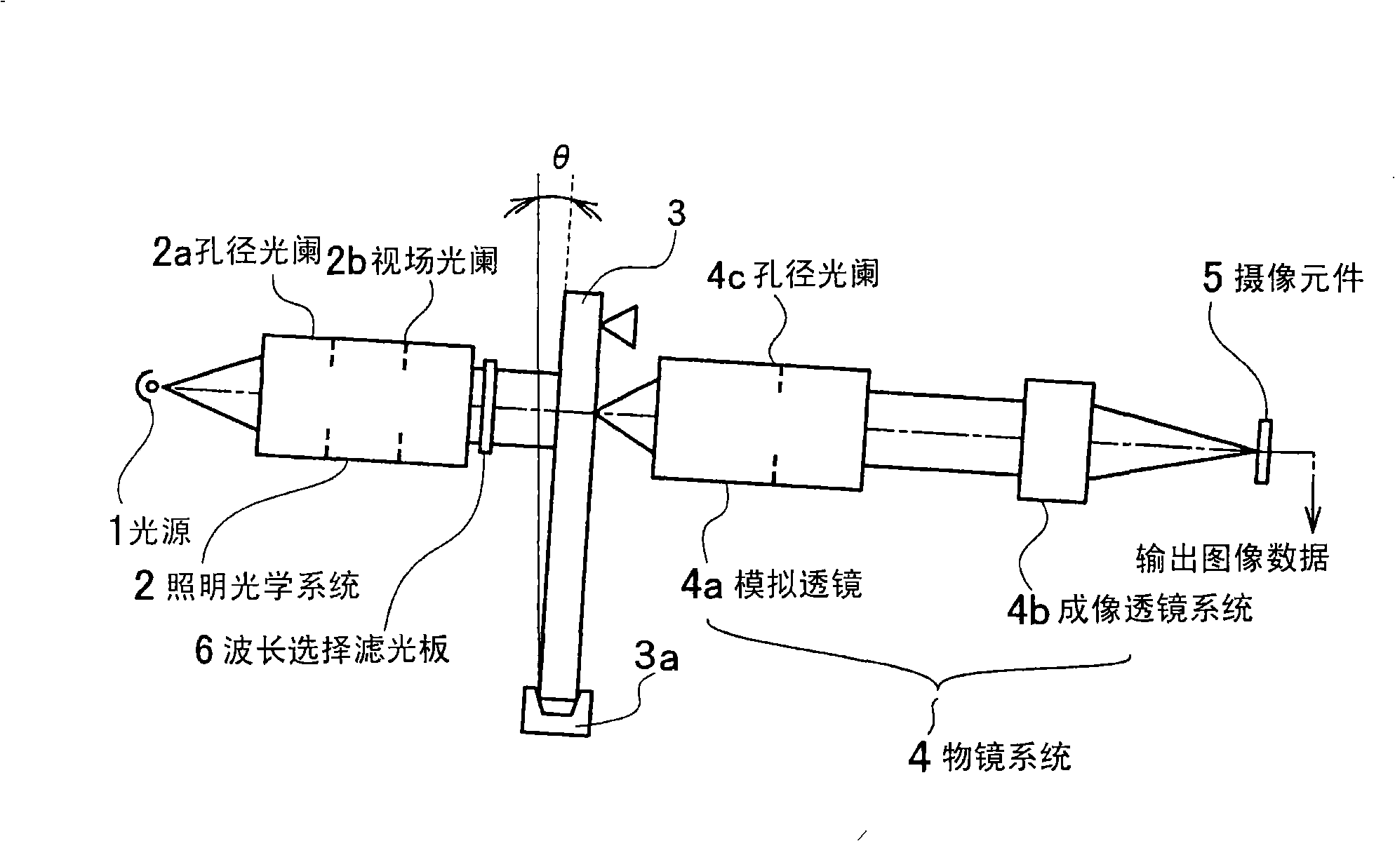
[0010]However, in this inspection method, sometimes it is difficult to fully reflect the exposure conditions of the exposure device used for actual exposure, that is, the spectral characteristics and resolution of the light source, etc.
In addition, the spectral sensitivity of the resist material used to form the resist film and the spectral sensitivity characteristics of the imaging device (CCD, etc.) used to acquire transmitted light data are caused by factors other than the exposure device, and it is difficult to match the conditions.

Method used


Image

  • Photomask testing method, photomask manufacture method, electronic component manufacture method, testing mask and testing mask set
  • Photomask testing method, photomask manufacture method, electronic component manufacture method, testing mask and testing mask set
  • Photomask testing method, photomask manufacture method, electronic component manufacture method, testing mask and testing mask set

Examples


Embodiment Construction

[0112] Hereinafter, preferred embodiments for carrying out the present invention will be described.

[0113] [Outline of the inspection method of the photomask of the present invention]

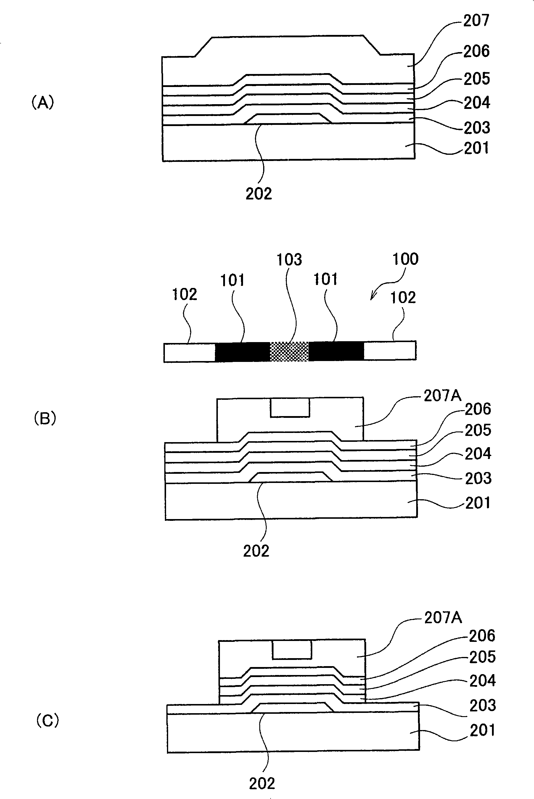
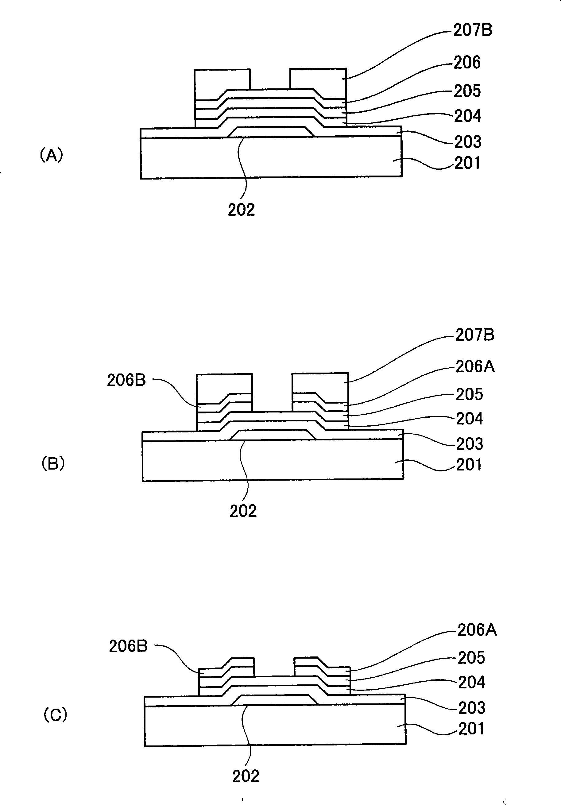
[0114] The inspection method of a photomask of the present invention is a method of exposing a transfer target body (glass substrate or silicon wafer) using an exposure device using a photomask having a predetermined pattern formed on a transparent substrate, and using the exposure device A method of inspecting a photomask by exposing an image transferred to a transfer target body by predicting the light intensity distribution captured by an imaging device.

[0115] Specifically, it includes a method in which an image similar to the image transferred to the transfer target body by exposure by the exposure device is imaged and inspected by an imaging device under exposure conditions similar to those of the exposure device; or a method using a simulation The detector quantitatively grasps the ...


PUM


Abstract

The invention relates to a detection method of a photo mask, a manufacturing method of a photo mask, a manufacturing method of an electronic member, a test mask and a test mask group; wherein, the test mask is used to undergo exposure, development, to acquire test resist pattern to be test to acquire actual exposure test pattern data; in addition, optical irradiation undergoes for the test mask under a specified optical condition to acquire light transmission pattern through imaging equipment, and further acquire light transmission test pattern data based on the same; the actual exposure test pattern data is compared to the light transmission test pattern data so as to set an optical condition based on the result of the compare, to undergo detection of the photo mask based on the light transmission pattern acquired through optical irradiation for the photo mask as the detection object.

Description

technical field [0001] The present invention relates to a photomask inspection method for inspecting the performance of a photomask used in the production of electronic components, a photomask production method including an inspection process based on the inspection method, and a photomask using the The manufacturing method of the electronic component of the photomask obtained by the manufacturing method, and the test mask and the test mask group applicable to the inspection method of the said photomask. [0002] In particular, the present invention relates to the manufacture of photomasks used in the manufacture of display devices represented by flat panel display devices (FPD), especially in the manufacture of liquid crystal display devices, such as in the manufacture of thin film transistors (TFTs), color filters ( CF) The inspection method used for the manufacture of a useful photomask, etc. are manufactured. Background technique [0003] Currently, regarding the inspec...

Claims


Application Information

Patent Timeline
IPC IPC(8): G03F1/14G03F1/00G03F7/20G01N21/956G03F1/84H01L21/027
CPCG03F1/44G03F1/84G03F7/7085H01L21/0274H01L21/0337H01L22/12
Inventor 中西胜彦吉田光一郎
Owner HOYA CORP
Learn More