Semiconductor device, led head and image forming apparatus
A semiconductor and substrate technology, applied in the field of semiconductor devices, LED heads and image forming devices, can solve the problem of reducing the heat dissipation effect
- Summary
- Abstract
- Description
- Claims
- Application Information
AI Technical Summary
Problems solved by technology
Method used
Image
Examples
Embodiment approach 1
[0087] In this embodiment, in order to minimize the distance between the main heating area and the substrate with high thermal conductivity, and effectively conduct heat energy to the outside of the device, the following structure is adopted:
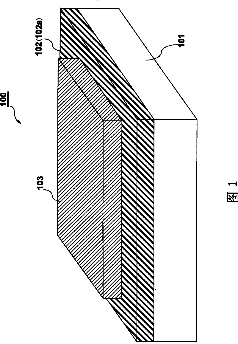
[0088] figure 1 It is a perspective view of the semiconductor device of the first embodiment.
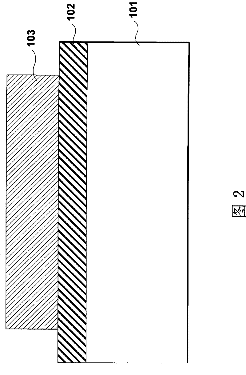
[0089] figure 2 It is a sectional view of the semiconductor device of the first embodiment.
[0090] As shown in the figure, in the semiconductor device 100 of Embodiment 1, the surface of the metal substrate 101 is covered with a surface coating layer 102 , and a semiconductor thin film layer 103 is bonded thereon. figure 2 The structure of the semiconductor thin film layer 103 is not indicated in the figure, and the semiconductor thin film layer 103 is a semiconductor thin film with semiconductor elements. Semiconductor elements include light-emitting diodes, semiconductor lasers (lasers), integrated circuits, sensors (sensors), light-...
Embodiment approach 2
[0171] In order to improve the luminous efficiency of the light-emitting element, this embodiment is based on the structure of Embodiment 1, and a metal layer with a higher light reflectivity is added on the metal substrate, and the following structure is adopted:
[0172] Figure 39 It is a plan view of the LED device of the second embodiment.
[0173] Figure 40 for Figure 39 Enlarged front view of the A-A section.
[0174] Refer below Figure 39 with Figure 40 A second embodiment will be described.
[0175] exist Figure 39 Among them, 411 is the GaAs layer (contact layer) on the first conductive side. 415 is the GaAs layer (contact layer) on the second conductive side. 417 is a second conductive side electrode. 417b is a wiring on the second conductive side, and 417c is a connection pad on the second conductive side. 418 is a first conductive side electrode. 418b is a first conductive side wiring, and 418c is a common wiring for connecting a plurality of first...
Embodiment approach 3
[0185]Different from Embodiment 1 and Embodiment 2, in this embodiment, a semiconductor thin film is bonded on an independent diamond-like carbon substrate for the purpose of further improving the heat dissipation effect.
[0186] Figure 42 It is a cross-sectional view of the semiconductor device of the third embodiment.
[0187] exist Figure 42 Among them, 501 is a diamond-like carbon substrate. 510 is a semiconductor thin film layer. The surface of the diamond-like carbon substrate preferably has the same flatness as the surface state described in the first embodiment. That is, Ra≤5nm, RPV≤10nm, preferably Ra≤3nm, RPV≤5nm. In addition, it is preferable that Rmax≤1 / 1000.
[0188] Figure 43 It is a sectional view of the LED element of the third embodiment.
[0189] Figure 43 It is a specific example of the semiconductor thin film layer 510 in the third embodiment. As shown in the figure, the LED element 450 of Embodiment 3 is the LED thin film element 410 of Embod...
PUM
| Property | Measurement | Unit |
|---|---|---|
| mean roughness | aaaaa | aaaaa |
| wavelength | aaaaa | aaaaa |
| thickness | aaaaa | aaaaa |
Abstract
Description
Claims
Application Information
 - Generate Ideas
- Intellectual Property
- Life Sciences
- Materials
- Tech Scout
- Unparalleled Data Quality
- Higher Quality Content
- 60% Fewer Hallucinations
Browse by: Latest US Patents, China's latest patents, Technical Efficacy Thesaurus, Application Domain, Technology Topic, Popular Technical Reports.
© 2025 PatSnap. All rights reserved.Legal|Privacy policy|Modern Slavery Act Transparency Statement|Sitemap|About US| Contact US: help@patsnap.com


