Arrayed optical address electric potential sensor chip and its manufacture method
A technology of a potential sensor and a manufacturing method, applied in the field of sensors, can solve the problems of long-term immersion, unsatisfactory noise suppression effect, pollution of sensitive areas, etc., and achieve the effects of shortening lifespan, facilitating positioning, and suppressing noise
- Summary
- Abstract
- Description
- Claims
- Application Information
AI Technical Summary
Problems solved by technology
Method used
Image

Examples
Embodiment 1
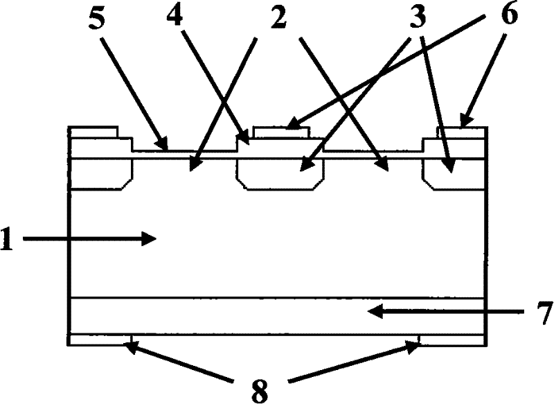
[0029] Such as Figure 4 As shown, the fabrication method of the arrayed light addressable potential sensor chip comprises the following steps:
[0030] 1) After the silicon substrate 1 is cleaned and dried, a thick oxide layer is grown by a thermal oxidation method, such as Figure 4 as shown in (a);
[0031] 2) On the oxide layer on the front side of the silicon substrate 1, a positive photoresist layer is coated by a spin method, and pre-baked in an oven at 80° C., then a mask is placed on the photoresist layer, and UV light is used to Exposure, the pattern of the mask plate is a rectangular array, the size of each rectangle is 1mm×1mm, and the distance between the rectangles is 1mm. After exposure, it is developed with a positive photoresist developer, and the film is hardened in an oven at 80°C. Etching with a silicon dioxide buffered etchant to remove the exposed oxide layer on the silicon substrate 1, then boiling the silicon substrate 1 in concentrated sulfuric acid ...
Embodiment 2
[0038] Such as Figure 4 As shown, the fabrication method of the arrayed light addressable potential sensor chip comprises the following steps:
[0039] 1) After the silicon substrate 1 is cleaned and dried, a thick oxide layer is grown by a thermal oxidation method, such as Figure 4 as shown in (a);
[0040] 2) On the oxide layer on the front side of the silicon substrate 1, a positive photoresist layer is coated by a spin method, and pre-baked in an oven at 100° C., then a mask is placed on the photoresist layer, and it is processed with ultraviolet light. Exposure, the pattern of the mask plate is a rectangular array, the size of each rectangle is 5mm×5mm, and the distance between the rectangles is 3mm. After exposure, it is developed with a positive photoresist developer, and the film is hardened in an oven at 100°C. Etching with a silicon dioxide buffered etchant to remove the exposed oxide layer on the silicon substrate 1, then boiling the silicon substrate 1 in conce...
Embodiment 3
[0047] Such as Figure 4 As shown, the fabrication method of the arrayed light addressable potential sensor chip comprises the following steps:
[0048] 1) After the silicon substrate 1 is cleaned and dried, a thick oxide layer is grown by a thermal oxidation method, such as Figure 4 as shown in (a);
[0049] 2) On the oxide layer on the front side of the silicon substrate 1, a positive photoresist layer is coated by a spin method, and pre-baked in an oven at 88° C., then a mask is placed on the photoresist layer, and UV light is used to Exposure, the pattern of the mask plate is a rectangular array, the size of each rectangle is 3mm×3mm, and the distance between the rectangles is 2mm. After exposure, it is developed with a positive photoresist developer, and the film is hardened in an oven at 88°C. Etching with a silicon dioxide buffered etchant to remove the exposed oxide layer on the silicon substrate 1, then boiling the silicon substrate 1 in concentrated sulfuric acid ...
PUM
| Property | Measurement | Unit |
|---|---|---|
| thickness | aaaaa | aaaaa |
| thickness | aaaaa | aaaaa |
| thickness | aaaaa | aaaaa |
Abstract
Description
Claims
Application Information
 - R&D
- Intellectual Property
- Life Sciences
- Materials
- Tech Scout
- Unparalleled Data Quality
- Higher Quality Content
- 60% Fewer Hallucinations
Browse by: Latest US Patents, China's latest patents, Technical Efficacy Thesaurus, Application Domain, Technology Topic, Popular Technical Reports.
© 2025 PatSnap. All rights reserved.Legal|Privacy policy|Modern Slavery Act Transparency Statement|Sitemap|About US| Contact US: help@patsnap.com