Silicon slice edge exposure system and its light intensity control method

An edge exposure and light intensity control technology, applied in the field of ultraviolet light exposure systems, can solve the problem of difficulty in accurately measuring exposure light intensity and other problems

Active Publication Date: 2008-07-16
SHANGHAI MICRO ELECTRONICS EQUIP (GRP) CO LTD
View PDF1 Cites 14 Cited by
  • Summary
  • Abstract
  • Description
  • Claims
  • Application Information

AI Technical Summary

Problems solved by technology

[0009] The purpose of the present invention is to solve the problem that it is difficult to accurately measure the exposure light intensity and precisely control the exposure dose in the traditional silicon wafer edge exposure system

Method used


Image

  • Silicon slice edge exposure system and its light intensity control method
  • Silicon slice edge exposure system and its light intensity control method
  • Silicon slice edge exposure system and its light intensity control method

Examples


Embodiment Construction

[0023] The specific embodiments of the present invention will be further described below in conjunction with the accompanying drawings.

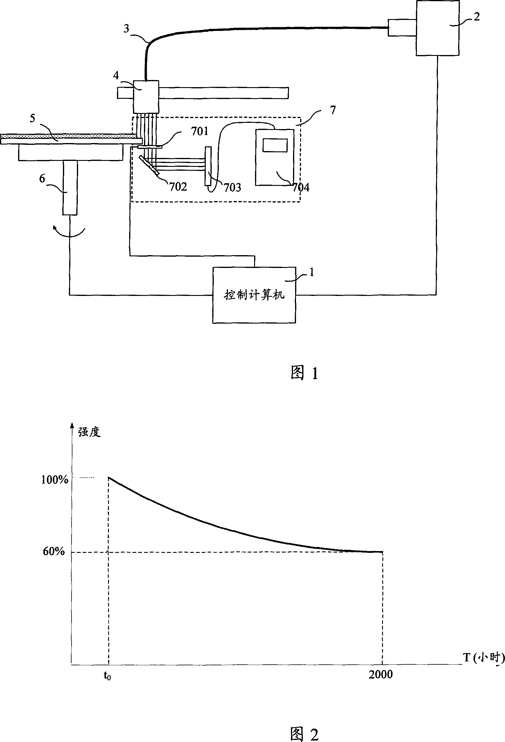
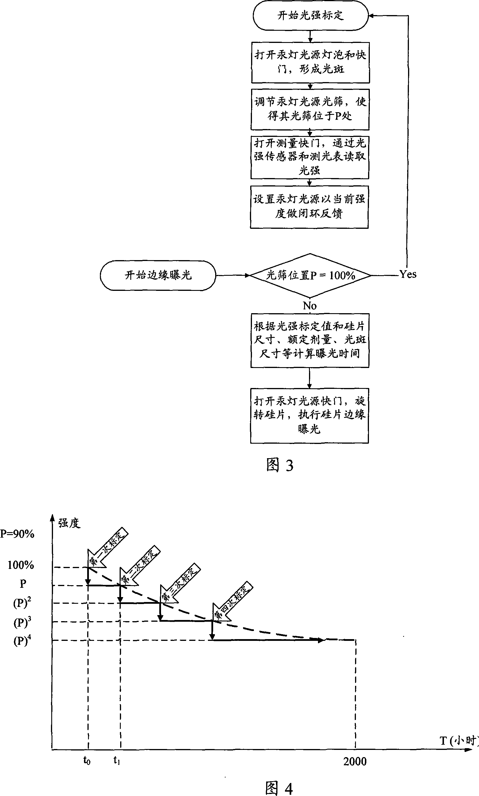
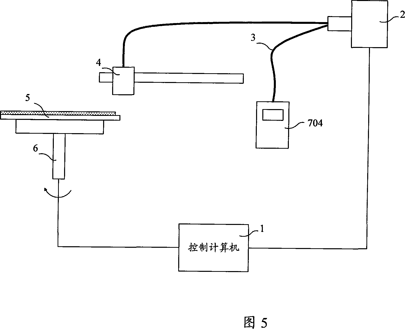
[0024] Figure 1 is a schematic diagram of the structure of the silicon wafer edge exposure system. The edge exposure system of the present invention is composed of a control computer 1 , a mercury lamp light source 2 , an optical fiber 3 , an imaging lens 4 , a silicon wafer carrier 6 and a light intensity control device 7 . The silicon wafer 5 coated with photoresist is placed on the silicon wafer carrying platform 6 . The light intensity control device 7 includes a measurement shutter 701 , a reflected light path 702 , a light intensity sensor 703 and a light meter 704 .

[0025] The control computer 1 controls the exposure light source 2 to switch on and off the light bulb, the shutter and set related parameters through the serial port. The exposure light source 2 can realize closed-loop feedback control based on its internal light inte...


PUM


Abstract

The invention provides a silicon wafer edge exposing system and a light intensity control method thereof, wherein the system comprises a rotatable silicon wafer bearing stage, an exposing light source and optical fiber, an imaging lens, a control computer and a light intensity control device; the method comprises the following steps that: through setting the position of a light sieve, the light intensity control device can calibrate exposing light intensity; the constant output of light intensity is controlled through the internal light intensity closed-loop feedback of the light source; through detecting the position of the light sieve, whether calibration is needed once more is judged; an exposing light source switch and the rotation time of a silicon wafer rotary stage are controlled through the calibrated data of light intensity. Adopting the system and the method can realize ladder-type constant output of light intensity, thereby making full use of the intensity of a mercury lamp light source and ensuring the constant output of light intensity within a certain time; meanwhile, the invention increases the efficiency and reliability of silicon wafer edge exposing process; in addition, the invention obtains the effect that a plurality of sets of silicon wafer edge exposing systems uses a set of photometric system; moreover, the invention further provides a simplified light intensity control device, thereby saving equipment cost.

Description

technical field [0001] The invention relates to an ultraviolet light exposure system, in particular to a silicon chip edge exposure system in semiconductor photolithography equipment and a light intensity control method thereof. Background technique [0002] In the semiconductor photolithography process, due to transmission and other reasons, the silicon wafer coated with photoresist often causes the photoresist on the edge of the silicon wafer to fall off, pollute, etc. These phenomena will have various effects on the subsequent process, resulting in chip defects. . Therefore, the photoresist at the edge of the silicon wafer needs to be removed. [0003] In the post-packaging of integrated circuits, the electroplating process is one of the important process steps. It uses the edge of the silicon wafer as the anode, and the electroplating window in the middle of the silicon wafer as the cathode, and then adds a certain DC working voltage between the cathode and anode. Throu...

Claims


Application Information

Patent Timeline
IPC IPC(8): G03F7/20
Inventor 谢威徐兵
Owner SHANGHAI MICRO ELECTRONICS EQUIP (GRP) CO LTD
Why Eureka
Try Eureka