
Oscillator and design method thereof

A technology for oscillators and oscillating signals, applied in instruments, static memory, single output arrangements, etc., can solve the problems of high power consumption and current consumption of ring oscillators, achieve large oscillation periods, simple design, and wide application range Effect

Active Publication Date: 2008-06-18
GIGADEVICE SEMICON (BEIJING) INC
View PDF0 Cites 7 Cited by
  • Summary
  • Abstract
  • Description
  • Claims
  • Application Information

AI Technical Summary

Problems solved by technology

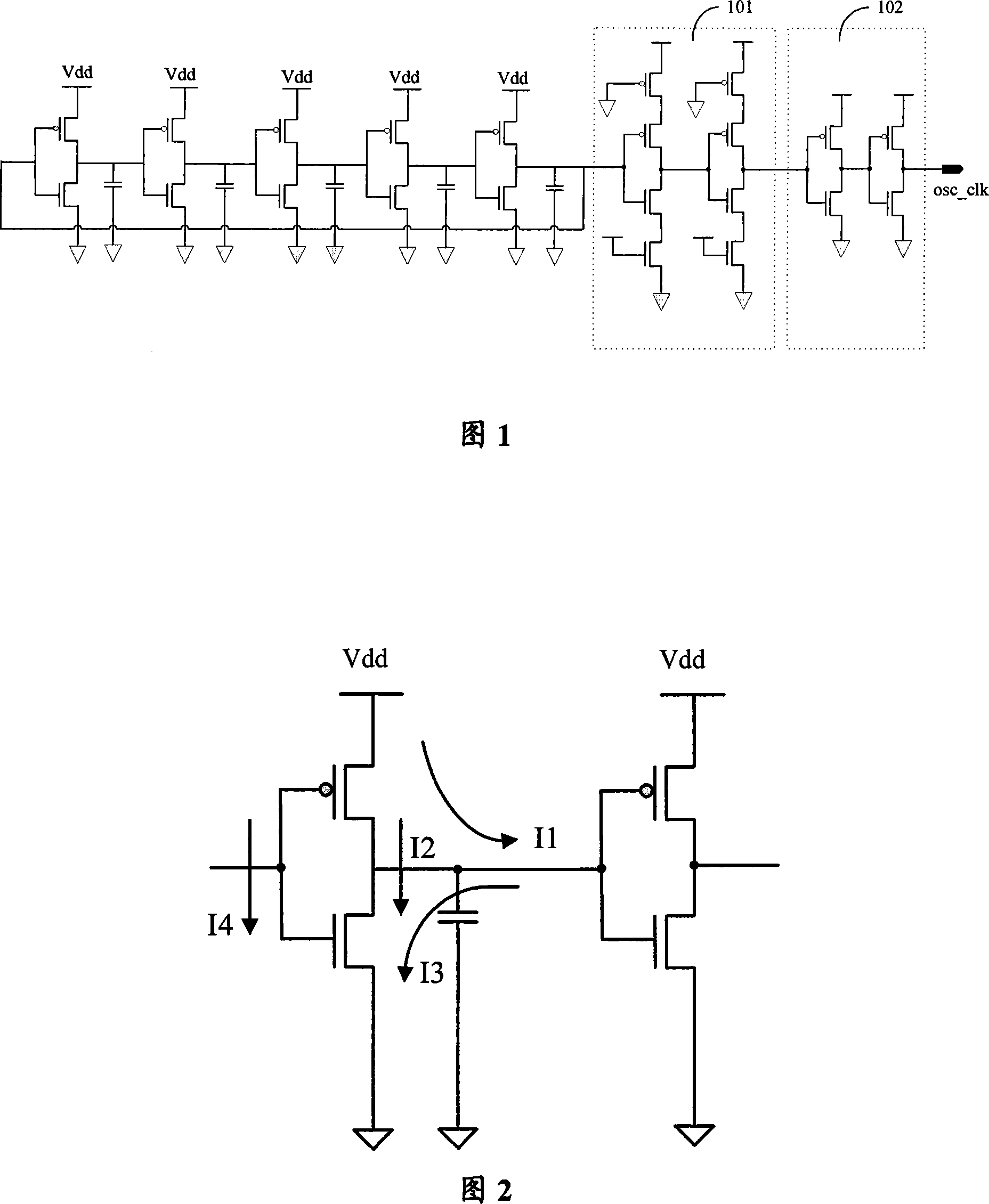
In addition, the buffer circuit 101 and the output circuit 102 in FIG. 1 also consume part of the current, which is also critical for the design of ultra-low power consumption
In summary, inverter-based ring oscillators consume a lot of power

Method used


Image

  • Oscillator and design method thereof
  • Oscillator and design method thereof
  • Oscillator and design method thereof

Examples


Embodiment Construction

[0090] Specific embodiments of the present invention will be described in detail below in conjunction with the accompanying drawings.

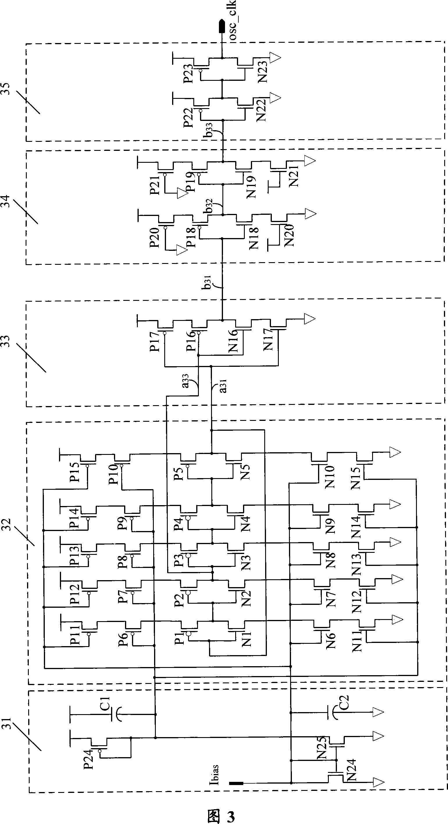
[0091] FIG. 3 is a gate-level circuit structure diagram of a low-power oscillator in the first embodiment of the present invention, which includes: a bias module 31 , a delay module 32 , a conversion module 33 , a buffer module 34 and an output module 35 .

[0092] The bias module 31 is used for inputting the bias current I bias A bias current is provided for the PMOS transistor group and the N-type Metal Oxide Semiconductor (NMOS, N type Metal Oxide Semiconductor) transistor group of the delay module 32 . Among them, NMOS transistors N24, N25 and PMOS transistor P24 will input the bias current I bias converted into the bias current required by the delay module 32.

[0093] The delay module 32 is configured to receive the bias current generated by the bias module, and generate an oscillating signal of a predetermined period according to the ...


PUM


Abstract

The invention discloses an oscillator and a design method thereof, comprising an offset module, a delaying module, a conversion module, a damping module and an output module; wherein, the offset module is used for generating an offset current according to an input signal; the delaying module is used for receiving the offset current which is generated by the offset module and generates the oscillation signals with scheduled periods according to the offset signal; the delaying module comprises a current source submodule, a variable resistance submodule and an inverter submodule; the maximum up-pulling current and the maximum down-pulling current of the delaying module are controlled by the power source submodule, thus controlling the power loss current of the delaying module; the delaying time of the delaying module is controlled by the variable resistance submodule; the gate capacitance of the delaying module is adjusted by the inverter submodule, thus controlling the power loss of the delaying module. The conversion module reduces the power loss of the oscillator by further reducing the DC current. The invention provides the oscillator which has simple structure, high efficiency, side application range and ultra-low power loss, and is especially suitable for low frequency application.

Description

technical field [0001] The invention mainly relates to the field of integrated circuit design, in particular to an oscillator and a design method thereof. Background technique [0002] As the basic circuit of the electronic system, the oscillator is used to generate various clock signals required by the system. The power consumption of the oscillator is relatively small for the dynamic power consumption during normal operation of the system. But when the system is in the standby state, the power consumption of the system is very small. If the oscillator is still working, its power consumption is very important as a component of the standby power consumption. Especially for battery-powered mobile systems, since standby power consumption is considered a key indicator of mobile system operation, oscillator power consumption, which is an important part of standby power consumption, is extremely important. [0003] Dynamic Random Access Memory (DRAM, Dynamic Random Access Memor...

Claims


Application Information

Patent Timeline
Patent Type & Authority Applications(China)
IPC IPC(8): H03K3/012H03K3/03H03K19/20H03K5/13G11C11/406H03K5/134H03K5/135
Inventor 朱一明胡洪
Owner GIGADEVICE SEMICON (BEIJING) INC
Learn More