Double face high-temperature superconducting film multi-layer structures and method for producing the same
A high-temperature superconducting thin film, multi-layer structure technology, applied in the usage of superconducting elements, the manufacture/processing of superconducting devices, superconducting devices, etc. effect of widening, improving texture, and enhancing film structure and properties
- Summary
- Abstract
- Description
- Claims
- Application Information
AI Technical Summary
Problems solved by technology
Method used
Image


Examples
Embodiment 1
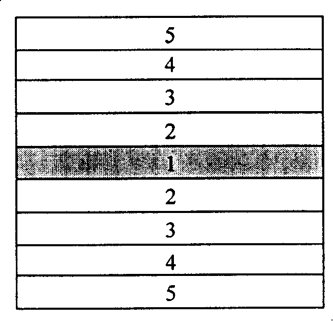
[0035] Such as figure 1 Shown is a schematic structural view of a large-area double-sided superconducting thin film prepared in one of the embodiments of the present invention. Among them, 1 is silicon single crystal double-sided polished substrate, 2 is metal Fe film, 3 is MgO film with biaxial texture, 4 is CeO 2 (100) film, 5 is YBCO superconducting film.
[0036] The silicon single crystal substrate is polished on both sides. Under vacuum and non-oxidizing conditions, a metal Fe thin film is deposited on the surface of a double-sided polished silicon single crystal substrate by radio frequency or direct current sputtering, and the prepared thickness is 100 nm.
[0037] A MgO metal oxide thin film layer (seed layer) with a thickness of 500nm was prepared by ion beam assisted deposition (Ion-Beam Aid Deposition) on the substrate with metal iron thin film deposited on both sides.
[0038] Epitaxial Growth of CeO on MgO Metal Oxide Thin Films Using RF Magnetron Sputtering ...
Embodiment 2
[0043] Such as figure 2 Shown is a schematic structural view of the large-area double-sided superconducting thin film prepared in Example 2 of the present invention. Among them, 1 is a high-temperature-resistant glass substrate polished on both sides, 2 is a metal Ni film, and 3 is YSZ with biaxial texture (that is, Y-stabilized ZrO 2 Thin film, its specific composition is: (Zr, Y)O 2 , Zr:Y=91:9) film, 5 is YBCO superconducting film.
[0044] Under vacuum and non-oxidizing conditions, a Ni film is deposited and prepared on the surface of a double-sided polished substrate by radio frequency or direct current sputtering, and the prepared thickness is 1 μm.
[0045]A 100nm biaxially textured YSZ film was prepared by ion beam-assisted deposition on a substrate with nickel metal film deposited on both sides. Then, a YBCO(001) film was epitaxially grown on the prepared YSZ film by DC magnetron sputtering, and the thickness of the YBCO film was 300nm. When preparing YBCO, the s...
Embodiment 3
[0047] Such as image 3 Shown is a schematic structural view of the large-area double-sided superconducting thin film prepared in Example 3 of the present invention. Among them, 1 is a double-sided polished ceramic substrate, 2 is a metal Ni film, 3 is a MgO film with biaxial texture, and 4 is CeO 2 Thin film, 5 is YBCO superconducting thin film.
[0048] Under vacuum and non-oxidizing conditions, a metal nickel film is deposited on the surface of a double-sided polished substrate by radio frequency or direct current sputtering, and the prepared thickness is 500nm.
[0049] A 300nm MgO film was prepared by ion beam-assisted deposition on the double-sided deposited metal film substrate; the prepared MgO film has the characteristics of biaxial texture, and CeO was grown epitaxially on the MgO by radio frequency magnetron sputtering 2 (100) oriented films with improved surface texture and φ scan half maximum width. CeO in this example 2 The thickness is 200nm. Then using DC ...
PUM
| Property | Measurement | Unit |
|---|---|---|
| thickness | aaaaa | aaaaa |
| thickness | aaaaa | aaaaa |
| thickness | aaaaa | aaaaa |
Abstract
Description
Claims
Application Information
 - R&D
- Intellectual Property
- Life Sciences
- Materials
- Tech Scout
- Unparalleled Data Quality
- Higher Quality Content
- 60% Fewer Hallucinations
Browse by: Latest US Patents, China's latest patents, Technical Efficacy Thesaurus, Application Domain, Technology Topic, Popular Technical Reports.
© 2025 PatSnap. All rights reserved.Legal|Privacy policy|Modern Slavery Act Transparency Statement|Sitemap|About US| Contact US: help@patsnap.com