Colorful optical filtering substrate and its manufacturing method, LCD panel and device
A technology of color filter substrate and liquid crystal display device, which is applied in optics, optical elements, nonlinear optics, etc., can solve problems affecting display characteristics, uneven brightness, and constant bright spots, etc., to improve side erosion and reduce critical dimensions Loss, improve the effect of acid resistance
- Summary
- Abstract
- Description
- Claims
- Application Information
AI Technical Summary
Problems solved by technology
Method used
Image

Examples
no. 1 example
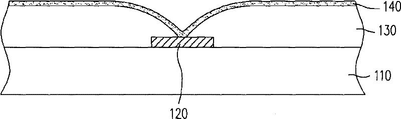
[0082] Figure 2A shows a schematic cross-sectional view of a liquid crystal display device according to a first embodiment of the present invention, and Figure 2B exhibit Figure 2A Schematic cross-section of the color filter substrate. Please refer to Figure 2A, the liquid crystal display device 10 of this embodiment includes a direct-type backlight module 200 and a liquid crystal display panel 300 , wherein the liquid crystal display panel 300 is disposed on the direct-type backlight module 200 . In addition, the direct type backlight module 200 includes a frame body 210, a plurality of light sources 220 and a diffusion plate (diffusion plate) 230, wherein the light sources 220 are disposed in the frame body 210, and the diffusion plate 230 is disposed on the frame body 210. . The light emitted by the light source 220 is emitted from the surface of the diffuser plate 230 to form a surface light source. Although the present embodiment adopts the direct type backlight ...
no. 2 example
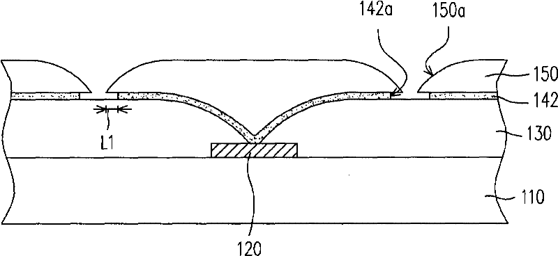
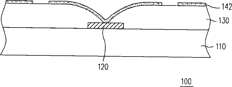
[0106] Figure 4A to Figure 4C A schematic cross-sectional view showing the manufacturing method of the color filter substrate according to the second embodiment of the present invention. Please refer to Figure 4A , this embodiment is similar to the above embodiment, the difference is that after forming the black matrix 3120 and the color filter layer 3130 on the transparent substrate 3110, an organic cover layer 4110 is formed on the transparent substrate 3110 to cover the black matrix 3120 and the color filter layer 3130. Color filter layer 3130. In addition, the method of forming the organic coating layer 4110 may be spin coating or spinless coating. In addition, the material of the organic cover layer 4110 can be a photoresist material; even a lower level organic cover layer 4110 can be used to improve the diffusion of pollutants in the color filter layer 3130 into the liquid crystal layer 330 to contaminate the liquid crystal. Then, an inorganic layer 3140 and a condu...
no. 7 example
[0122] Figure 6A to Figure 6C A schematic cross-sectional view showing a manufacturing method of a color filter substrate according to a seventh embodiment of the present invention is shown. Please refer to Figure 6A , this embodiment is similar to the above-mentioned first embodiment, the difference is that: after the black matrix 3120 and the color filter layer 3130 are formed on the transparent substrate 3110 , the conductive layer 3150 is formed on the color filter layer 3130 . Please refer to Figure 6B , forming a patterned photoresist layer 3160 on the conductive layer 3150, wherein the patterned photoresist layer 3160 has a plurality of slits 3160a. Then, the conductive layer 3150 is etched using the patterned photoresist layer 3160 as a mask to form a patterned conductive layer 3152, wherein the patterned conductive layer 3152 has a plurality of slits 3152a.
[0123] Please refer to Figure 6C , after forming the patterned conductive layer 3152, the patterned ph...
PUM
| Property | Measurement | Unit |
|---|---|---|
| thickness | aaaaa | aaaaa |
| thickness | aaaaa | aaaaa |
| thickness | aaaaa | aaaaa |
Abstract
Description
Claims
Application Information
 - Generate Ideas
- Intellectual Property
- Life Sciences
- Materials
- Tech Scout
- Unparalleled Data Quality
- Higher Quality Content
- 60% Fewer Hallucinations
Browse by: Latest US Patents, China's latest patents, Technical Efficacy Thesaurus, Application Domain, Technology Topic, Popular Technical Reports.
© 2025 PatSnap. All rights reserved.Legal|Privacy policy|Modern Slavery Act Transparency Statement|Sitemap|About US| Contact US: help@patsnap.com