Manufacturing method for blind hole of insulating substrate for electronic apparatus

A technology for insulating substrates and manufacturing methods, which is applied in the direction of insulators, chemical instruments and methods, and photoplate-making processes for patterned surfaces, and can solve problems such as side etching, poor adhesion between resist films and glass substrates, etc.

Inactive Publication Date: 2016-01-20
INTERFACE OPTOELECTRONICS SHENZHEN +1
View PDF4 Cites 6 Cited by
  • Summary
  • Abstract
  • Description
  • Claims
  • Application Information

AI Technical Summary

Problems solved by technology

However, the poor adhesion between the resist film and the glass substrate often causes the etching solution to flow between the resist film and the glass substrate, resulting in obvious side etching

Method used


Image

  • Manufacturing method for blind hole of insulating substrate for electronic apparatus
  • Manufacturing method for blind hole of insulating substrate for electronic apparatus
  • Manufacturing method for blind hole of insulating substrate for electronic apparatus

Examples


Embodiment Construction

[0031] Next, the present invention will be described in detail with embodiments and accompanying drawings. In the drawings or descriptions, the same symbols or numbers are used for similar or identical parts. In the drawings, the shapes or thicknesses of the embodiments may be exaggerated for simplification or convenient labeling, and parts of the elements in the drawings will be described in words. It can be understood that elements not shown or described can be in various forms known to those of ordinary skill in the art. This embodiment is illustrated in schematic cross-section of an idealized embodiment (and intermediate structures) of the invention, and reasonable variations in fabrication methods, shapes and / or tolerances will be contemplated by those skilled in the art. Therefore, the embodiments of the present invention should not be construed as limiting the scope of the present invention claimed.

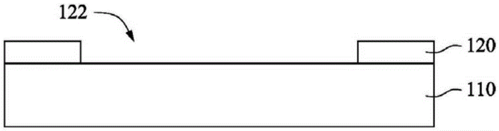
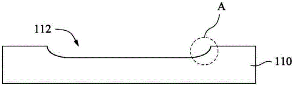
[0032] Figure 1A ~ 1C It is a sectional view of various stages of f...


PUM


Abstract

The invention relates to a manufacturing method for a blind hole of an insulating substrate for an electronic apparatus. The manufacturing method comprises the following steps of forming a patterned photoresist layer on the insulating substrate, wherein an opening is formed in the patterned photoresist layer, and a part of the insulating substrate is exposed out of the opening; performing a wet etching process to move the exposed insulating substrate, wherein the blind hole is formed in the opening. The manufacturing method can dramatically reduce the side etching phenomenon of an etching liquid and reduce the residual width in the edge of the blind hole so as to further improve the precision degree of the blind hole formed by the wet etching method.

Description

technical field [0001] The invention relates to a method for manufacturing a blind hole of an insulating substrate of an electronic device, in particular to a method for manufacturing a blind hole of an insulating substrate by using a photoresist layer. Background technique [0002] In the past, physical drilling was usually used to form blind holes on glass substrates for electronic devices, but this method will generate a lot of dust particles, which will cause difficulties in subsequent processing, such as problems such as ink coatings that cannot be applied. . Therefore, in recent years, chemical etching has been used to form blind holes on glass substrates. [0003] In order to selectively etch blind holes in a specific area on the glass substrate, a resist film is usually attached on the glass substrate first, and then the area to be etched on the glass substrate is cut out by laser, and then the glass substrate is immersed in the etching solution to form blind vias ...

Claims


Application Information

Patent Timeline
Patent Type & Authority Applications(China)
IPC IPC(8): H01L21/48
CPCH01B19/04C03C15/00C09K13/04C09K13/08G03F7/0041H01B3/088H01L21/4803
Inventor 张俊德郭毓弼刘忠武庄伟仲
Owner INTERFACE OPTOELECTRONICS SHENZHEN
Why Eureka
Try Eureka