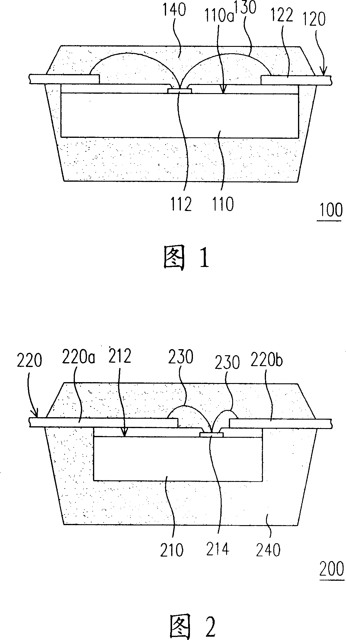
Chip packaging structure
A chip packaging structure, chip technology, applied in the direction of electrical components, electrical solid devices, circuits, etc., can solve the problems of easy-to-collapse electrical properties, long bonding wire length, low product yield, etc., to reduce the probability of collapse and reduce short-circuit long effect
- Summary
- Abstract
- Description
- Claims
- Application Information
AI Technical Summary
Problems solved by technology
Method used
Image
Examples
Embodiment Construction
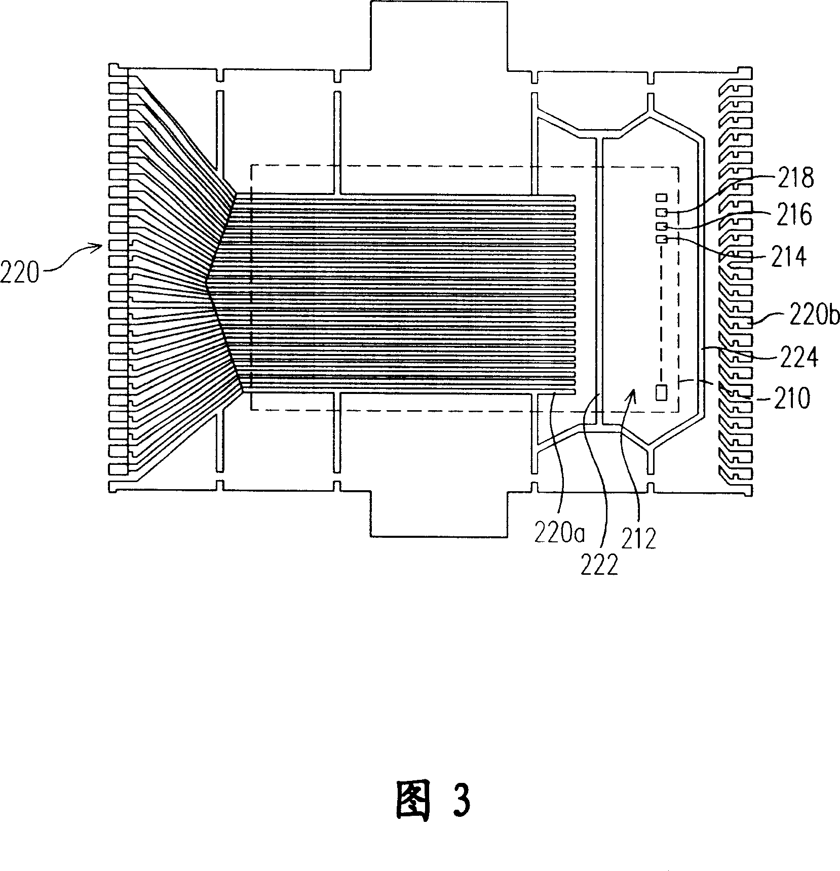
[0044] FIG. 2 is a schematic cross-sectional view of a chip packaging structure according to an embodiment of the present invention. Please refer to FIG. 2 , the chip packaging structure 200 includes a chip 210 , a lead frame 220 , a plurality of first bonding wires 230 and an encapsulant 240 . The chip 210 has an active surface 212 and a plurality of first pads 214 disposed on the active surface 212 , and the first pads 214 are located on one side of the active surface 212 . In more detail, the first pads 214 are adjacent to one side of the active surface 212 .
[0045] The chip 210 is fixed under the lead frame 220 . The lead frame 220 has a plurality of first inner leads 220a and a plurality of second inner leads 220b, wherein the first inner leads 220a are located on the active surface 212, and each first inner lead 220a is connected to each second inner lead 220b. One end of the inner pin 220 b is located on the periphery of the first pads 214 .
[0046] The first bond...
PUM
 Abstract
Description
Claims
Application Information
 - R&D
- Intellectual Property
- Life Sciences
- Materials
- Tech Scout
- Unparalleled Data Quality
- Higher Quality Content
- 60% Fewer Hallucinations
Browse by: Latest US Patents, China's latest patents, Technical Efficacy Thesaurus, Application Domain, Technology Topic, Popular Technical Reports.
© 2025 PatSnap. All rights reserved.Legal|Privacy policy|Modern Slavery Act Transparency Statement|Sitemap|About US| Contact US: help@patsnap.com


