Multilayer printed circuit board
A multi-layer printing and circuit board technology, applied in the direction of printed circuit parts, circuits, printed circuits connected with non-printed electrical components, etc., can solve problems such as reduced reliability, inability to obtain electrical connections, position deviation, etc., to achieve Effect of improving electrical conductivity and adhesion
- Summary
- Abstract
- Description
- Claims
- Application Information
AI Technical Summary
Problems solved by technology
Method used
Image
Examples
Embodiment 1
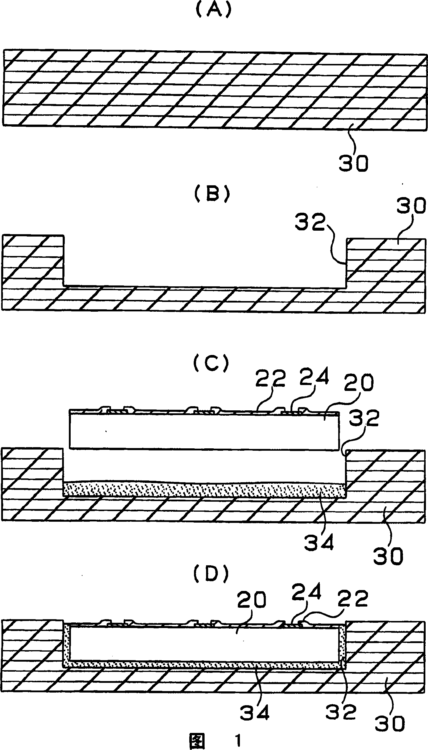
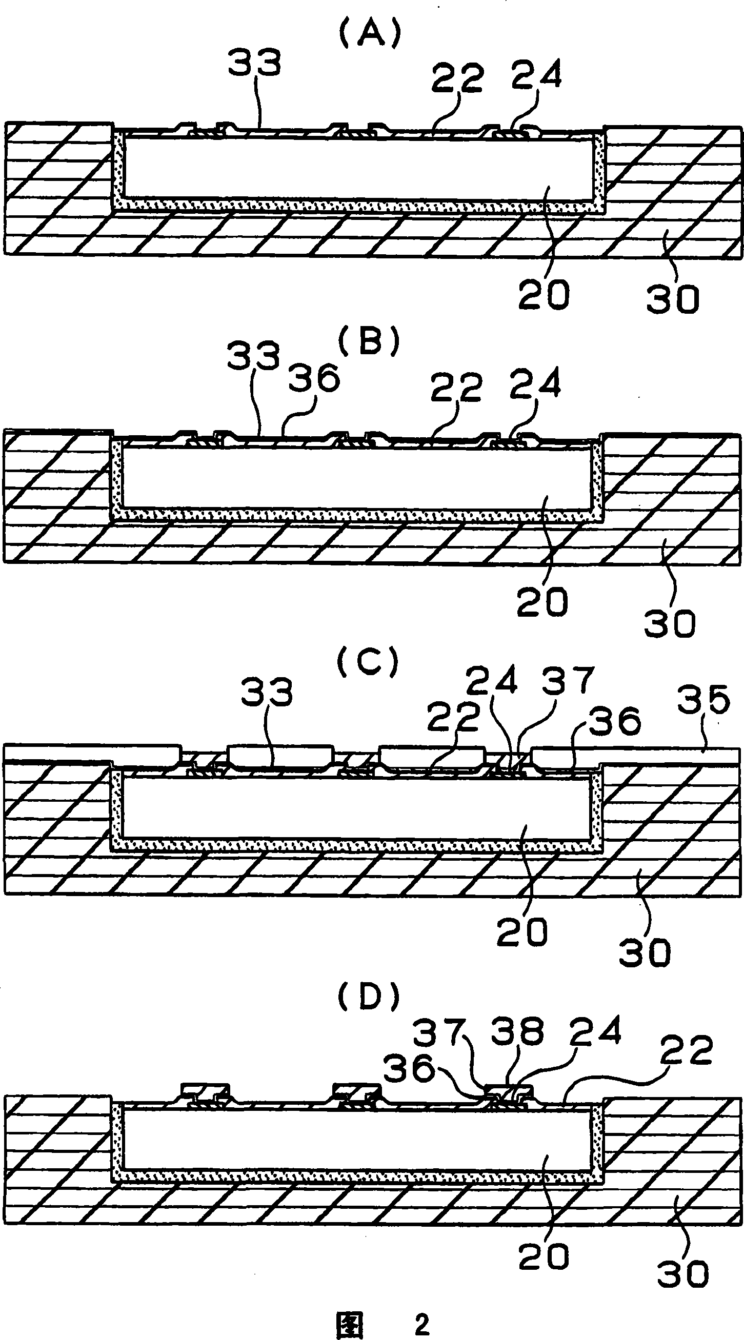
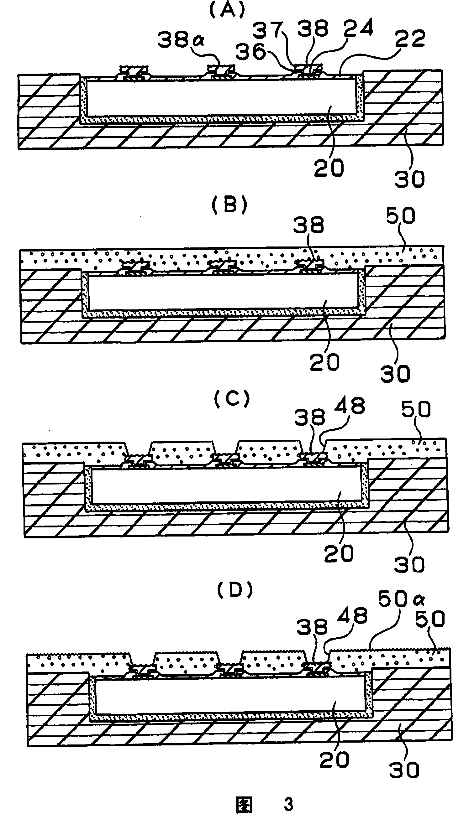
[0104] First, the configuration of the multilayer printed wiring board according to the first embodiment of the present invention will be described with reference to the cross section of the multilayer printed wiring board 10 shown in FIG. 6 .
[0105] The multilayer printed circuit board shown in Fig. 6 is composed of a core substrate 30 accommodating an IC chip 20, an interlayer resin insulating layer 50, and an interlayer resin insulating layer 150. On the interlayer resin insulating layer 50, a The through hole 60 and the conductive circuit 58 are formed on the interlaminar resin insulating layer 150 , and the through hole 160 and the conductive circuit 158 are formed.
[0106] The IC chip 20 is covered with a passivation film 24 , and a die pad 24 constituting an output terminal is arranged in an opening of the passivation film 24 . Over the die pad 24 made of aluminum, a transition layer 38 is formed. The transition layer 38 is composed of three layers of the first th...
Embodiment 2
[0208] Next, the structure of the multilayer printed wiring board according to the second embodiment of the present invention will be described with reference to the cross section of the multilayer printed wiring board shown in FIG. 18 .
[0209] The multilayer printed circuit board 210 shown in FIG. 18 is composed of a core substrate 230 accommodating an IC chip 220 , an interlayer resin insulating layer 250 , and an interlayer resin insulating layer 350 . The through hole 260 and the conductive circuit 258 are formed on the interlayer resin insulating layer 250 , and the through hole 360 and the conductive circuit 358 are formed on the interlayer resin insulating layer 350 .
[0210] A passivation film 224 is covered on the IC chip 220 , and a die pad 224 constituting an output terminal and a positioning mark 223 are arranged in an opening of the passivation film 224 . On top of the pad 224, a transition layer 238 mainly composed of copper is formed.
[0211] On the inter...
Embodiment 3
[0243] Next, the structure of the multilayer printed wiring board according to the third embodiment of the present invention will be described with reference to the cross section of the multilayer printed wiring board 410 shown in FIG. 26 .
[0244] The multilayer printed circuit board 410 shown in FIG. 26 is composed of a core substrate 430 accommodating an IC chip 420 , an interlayer resin insulating layer 450 , and an interlayer resin insulating layer 550 . The through hole 460 and the conductive circuit 458 are formed on the interlayer resin insulating layer 450 , and the through hole 560 and the conductive circuit 558 are formed on the interlayer resin insulating layer 550 .
[0245] The IC chip 420 is covered with an IC protective film (passivation+polyimide) 422, and an aluminum die pad 424 constituting an output terminal is arranged in the opening of the IC protective film 422. On the surface, an oxide coating film 426 is formed. On the die pad 424, a transition layer ...
PUM
| Property | Measurement | Unit |
|---|---|---|
| Diameter | aaaaa | aaaaa |
| Current density | aaaaa | aaaaa |
| Thickness | aaaaa | aaaaa |
Abstract
Description
Claims
Application Information
 - R&D
- Intellectual Property
- Life Sciences
- Materials
- Tech Scout
- Unparalleled Data Quality
- Higher Quality Content
- 60% Fewer Hallucinations
Browse by: Latest US Patents, China's latest patents, Technical Efficacy Thesaurus, Application Domain, Technology Topic, Popular Technical Reports.
© 2025 PatSnap. All rights reserved.Legal|Privacy policy|Modern Slavery Act Transparency Statement|Sitemap|About US| Contact US: help@patsnap.com


