
Fixer andits scanning electronic microscope for testing sample

A technology for electron microscopes and fixtures, which is applied in microscopes, semiconductor/solid-state device testing/measurement, circuits, etc. It can solve problems such as low test efficiency, sample drop, and image blurring, so as to improve sample manufacturing efficiency and speed. The effect of simple structure

Inactive Publication Date: 2007-09-05
SEMICON MFG INT (SHANGHAI) CORP +1
View PDF1 Cites 24 Cited by
  • Summary
  • Abstract
  • Description
  • Claims
  • Application Information

AI Technical Summary

Problems solved by technology

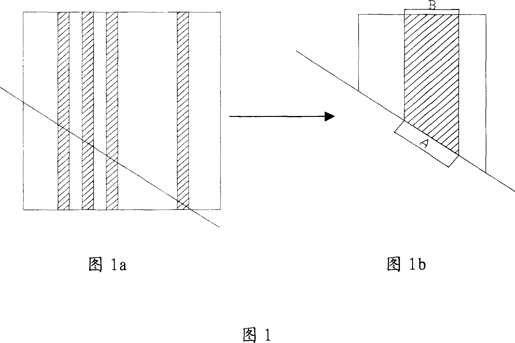
After the sample is ground, it is measured and analyzed by SEM, but since SEM uses electron beam scanning, it will bring heat to the sample, which will cause the temperature of the sample to rise, making the adhesion between the sample and the fixture weak
Therefore, when the cross-section of the sample is scanned by SEM, the cross-section often produces slight jitter or vibration due to weak adhesion. Very slight vibration will cause the image generated by SEM scanning to be blurred and unclear, and accurate data measurement cannot be completed. , resulting in inefficient testing
[0010] Furthermore, with the existing fixtures, during the grinding process, the sample often falls from the fixtures due to the grinding force or high-speed grinding, which leads to the waste of all previous efforts in the sample preparation process.

Method used


Image

  • Fixer andits scanning electronic microscope for testing sample
  • Fixer andits scanning electronic microscope for testing sample
  • Fixer andits scanning electronic microscope for testing sample

Examples


Embodiment Construction

[0032] The core idea of ​​the present invention is to change the situation in the prior art that the test sample is adhered to the fixing device by using hot melt to achieve fixation, and to realize the fixation by mechanically pressing the fixed wall and the movable wall, so that the test sample can be avoided. Vibration during electron beam scanning improves the quality of SEM scanning images; and because the distance between the fixed wall and the movable wall is adjustable, multiple test samples can be fixed at the same time to improve test efficiency.

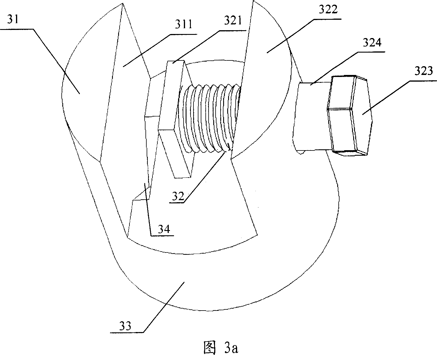
[0033] Referring to FIG. 3 , it is the first embodiment of the test sample fixing device of the present invention. Fig. 3a is a three-dimensional structure diagram of the first embodiment. Fig. 3b is a perspective view of the structure of the first embodiment, showing the internal and bottom structures invisible from the front with light-colored lines.

[0034]The test sample fixing device of the present invention is main...


PUM


Abstract

The invention is concerned with the fixing equipment for testing sample, which is used for test semiconductor chip, it includes: the fixing part, the compacted part and the base; the fixing part sets on the base that is with the fixing wall plumbing with the base, the compacted part consists of the active wall that plumbs with the base; forms the space between the fixing wall, the active wall ad the base that is used for fixing the testing sample. The invention is: improving the SEM imaging quality because the sample fixes on the fixing equipment and will not appearing vibrate during the scanning; improving the productivity and testing speed because the width of the sample is adjustable, which provides a multiple production.

Description

technical field [0001] The invention relates to the field of semiconductor chip analysis, in particular to a sample fixing device on a scanning electron microscope sample stage during the preparation and analysis of test samples. Background technique [0002] With the development of semiconductor integrated circuits, electron microscopes are more and more widely used in the microstructure analysis of products. IC (Integrated Circuit) manufacturing is basically built up by layers of patterns, and in order to understand the structure of the stacked patterns to improve the process or solve the failure problem in the process, it is often observed through an electron microscope by using a destructive cutting method , while cutting the cross section (CROSS SECTION) and observing the (crystal garden) cross section are the most basic means to detect the quality of the process. Electron microscopes generally include scanning electron microscope SEM (Scanning Electron Microscopy), tr...

Claims


Application Information

Patent Timeline
Patent Type & Authority Applications(China)
IPC IPC(8): H01J37/20H01J37/28H01L21/66G02B21/34
Inventor 陈险峰葛挺锋秦天邹丽君
Owner SEMICON MFG INT (SHANGHAI) CORP
Learn More