Printed circuit board for semiconductor package and method of manufacturing the same
A technology of printed circuit boards and semiconductors, which is applied in the fields of printed circuit manufacturing, printed circuits, printed circuits, etc., and can solve the problems of pre-soldering with a pitch of 120 μm or less and high cost in the screen printing method
- Summary
- Abstract
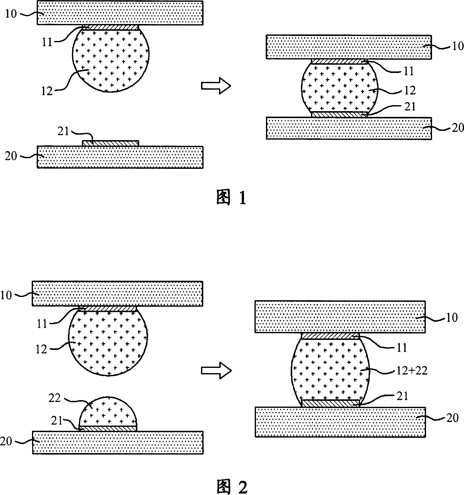
- Description
- Claims
- Application Information
AI Technical Summary
Problems solved by technology
Method used
Image

Examples
Embodiment 1
[0070] In the product as shown in FIG. 7, all solder parts, bump parts, and wire bond parts (with camera-recognizable marks and mold gates for molding after mounting) are tin-plated. In particular, the pitch of the bump portion is set in the range of 40˜200 μm, and the thickness of the plating layer is changed according to the pitch. In this embodiment, in the case of a pitch of 100 μm, since the bump copper circuit spacing is small, around 30 μm, tin plating is performed to a target thickness of 10 μm. To this end, an electroplating process was performed at 25° C. and 1.0 ASD for 25 min using a PC-MT electroplating solution obtained from Incheon Chemical in Korea, and the resulting plating layer contained at least 99% pure tin. In addition, the electroplating process was performed at 25° C. and 3 ASD for 12 min using UTB-TS 140 electroplating solution obtained from Ishihara Chemical in Japan, and the resulting plating layer contained 97.5% Sn and 2.5% Ag. Once the PCB thus f...
Embodiment 2
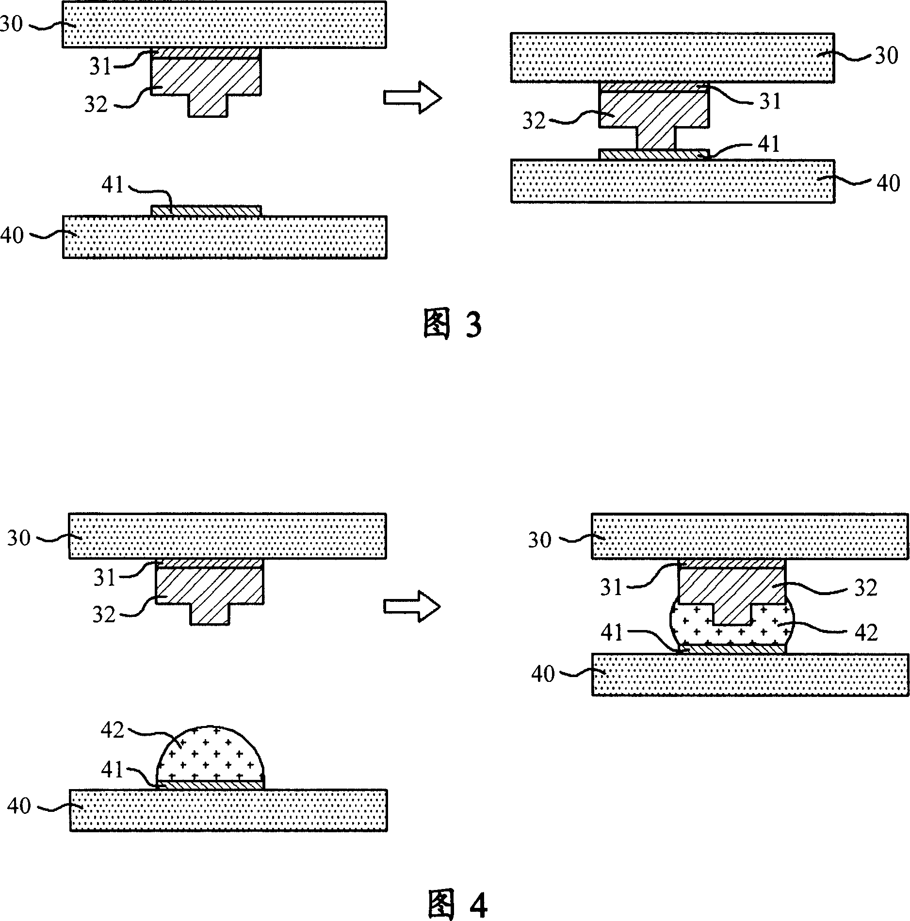
[0072] In the product shown in Fig. 8, among the soldering part, the bump part, and the wire bonding part (having a mark recognizable by a camera and a mold gate for molding after mounting), only the bump part Perform tin plating. Except for the bump part, nickel and gold plating is performed on the copper pad. Therefore, the bump portion is covered by the dry film so as not to be plated. Subsequently, when the bump portion is tin-plated, the portion of the substrate other than the bump portion is masked with a dry film so that the nickel and gold plated portion is not tin-plated. The thickness of the nickel plating layer is 2 to 20 μm, which is as thick as a general nickel plating layer. In particular, the pitch of the bump portion is set in the range of 40˜200 μm, and the thickness of the plating layer is changed according to the pitch. In this embodiment, in the case of a pitch of 100 μm, since the bump copper circuit spacing is small, around 30 μm, tin plating is perfor...
Embodiment 3
[0074] In the product shown in FIG. 9, among the soldering part, the bump part, and the wire bonding part (having a mark recognizable by a camera and a mold gate for molding after mounting), only the bump part Perform tin plating. All copper pads are plated with nickel and gold. Subsequently, when the bump portion is tin-plated, a dry film is used to mask the portion of the substrate other than the bump portion so that nickel and gold plating and subsequent tin plating are formed only on the bump portion. In particular, the pitch of the bump portion is set in the range of 40˜200 μm, and the thickness of the plating layer is changed according to the pitch. In the present embodiment, in the case of a 100 μm pitch, since the bump copper circuit interval is small, around 30 μm, the nickel plating layer is formed to a thickness of 1.0 μm, which is smaller than that of a normal nickel plating layer. In addition, tin plating was performed to a target thickness of 10 μm. To this en...
PUM
 Abstract
Description
Claims
Application Information
 - R&D
- Intellectual Property
- Life Sciences
- Materials
- Tech Scout
- Unparalleled Data Quality
- Higher Quality Content
- 60% Fewer Hallucinations
Browse by: Latest US Patents, China's latest patents, Technical Efficacy Thesaurus, Application Domain, Technology Topic, Popular Technical Reports.
© 2025 PatSnap. All rights reserved.Legal|Privacy policy|Modern Slavery Act Transparency Statement|Sitemap|About US| Contact US: help@patsnap.com