Diamond cone and its making process
A diamond cone and diamond technology, which is applied in the field of diamond cone tip materials and its production, can solve the problems of inability to obtain electrical information and shape information, diamond tip is not wear-resistant, and has little potential for mechanical application, so as to achieve excellent electrical and The effects of mechanical properties, controllable hardness, and stable electrical conductivity
- Summary
- Abstract
- Description
- Claims
- Application Information
AI Technical Summary
Problems solved by technology
Method used
Image
Examples
Embodiment 1
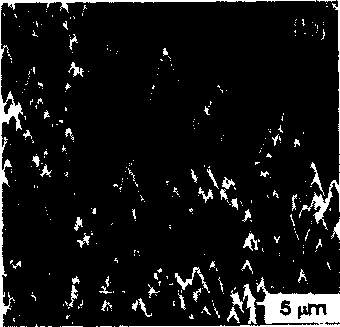
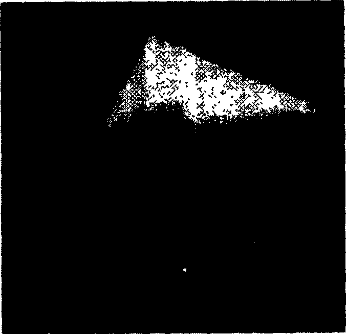
[0048] The specific structure of the diamond cone tip of the present embodiment refers to the attached Figure 5 (a); The diamond tip has an aspect ratio of 5, a tip curvature radius of 100 nanometers, and a bottom diameter of 4 microns.
[0049] refer to Figure 4 a-4f, the method of the present invention is described in detail according to its flow chart.
[0050] 1. On the surface of the single crystal silicon substrate 2, use a glue leveler to spin and coat a layer of PMMA photoresist with a thickness of about 200-300 nanometers as the protective material layer 1 with a concentration of 5%. The coating conditions are: rotating speed 4000 rpm, spin coating time is 1 minute;
[0051] 2. Put the silicon substrate 2 coated with the protective material layer 1 into the cavity of the focused ion beam system, and use the ion beam to etch a conical hole 3 with a diameter of 4 microns and a depth of 20 microns on the silicon wafer , that is, to obtain the silicon template 9; the...
Embodiment 2
[0056] The specific structure of the planar diamond tip of the present embodiment can be found in Figure 5 (b): The diamond cone tip has an aspect ratio of 6.75, a tip curvature radius of about 100 nanometers, and a bottom diameter of 2 microns.
[0057] refer to Figure 4 a-4f, the difference between this embodiment and embodiment 1 is that the gas-assisted ion beam etching technology is used to etch a conical hole 3 with a diameter of 2 microns and a depth of 13.5 microns to obtain a silicon template 9 . The etching process parameters: ion source voltage (30KV), ion beam current (1nA), beam spot spacing (50% of the beam spot diameter), and beam current residence time (1 microsecond) were not changed. All the other conditions are with embodiment 1. The diamond tip ( Figure 5 (b)) The upper part is conical, and there is an obvious step in the middle part, which is beneficial to the improvement of the overall strength. When the diameter of the etched hole is greater than...
Embodiment 3
[0059] The specific structure of the diamond cone tip of the present embodiment refers to the attached Figure 5 (c), the diamond cone tip has an aspect ratio of 7.7, a tip curvature radius of 30 nanometers, and a bottom diameter of 1 micron.
[0060] refer to Figure 4 a-4f, the difference between the method of the diamond tip made in the present embodiment and the embodiment 1 is that the gas-assisted ion beam is used in the present embodiment to etch a conical hole 3 with a diameter of 1 micron and a depth of 7.7 microns, i.e. Silicon template 9 was obtained. Etching process parameters: ion source voltage (30KV), ion beam current (3nA), beam spot spacing (150% of beam spot diameter), and beam current residence time (0.2 microseconds) have all been changed. The diamond tip ( Figure 5 (c)) In addition to having a large base, the top is tapered and conical. When the diameter of the etched hole is greater than 1 micron, its relative shape does not change with the diameter o...
PUM
| Property | Measurement | Unit |
|---|---|---|
| diameter | aaaaa | aaaaa |
Abstract
Description
Claims
Application Information
 - R&D
- Intellectual Property
- Life Sciences
- Materials
- Tech Scout
- Unparalleled Data Quality
- Higher Quality Content
- 60% Fewer Hallucinations
Browse by: Latest US Patents, China's latest patents, Technical Efficacy Thesaurus, Application Domain, Technology Topic, Popular Technical Reports.
© 2025 PatSnap. All rights reserved.Legal|Privacy policy|Modern Slavery Act Transparency Statement|Sitemap|About US| Contact US: help@patsnap.com


