Atoll static release device

A technology of static electricity and resistance area, applied in circuits, electrical components, semiconductor devices, etc., can solve the problems of chip damage, weak anti-reverse bias electrostatic damage ability, etc., so as to increase manufacturing cost and enhance anti-reverse bias electrostatic damage. , Enhance the effect of anti-reverse bias electrostatic damage ability

Active Publication Date: 2009-03-11
LAND MARK OPTOELECTRONICS
View PDF2 Cites 0 Cited by
  • Summary
  • Abstract
  • Description
  • Claims
  • Application Information

AI Technical Summary

Problems solved by technology

[0002] Press, the chip of conventional photodetector (see figure 1 and figure 2 ), the chip is mainly composed of P-type metal layer 1, light-receiving area 2, dielectric layer 3, N - Type semiconductor layer 4, P-type semiconductor region 41, i-type light absorbing layer 5, N-type buffer layer 6, N-type substrate 7, and N-type metal layer 8: Among them, when there is a large amount of static electricity on the chip surface, a large amount of static electricity runs through The middle area of ​​the chip will cause damage to the chip. Apply reverse bias static electricity to simulate a large amount of static electricity passing through the chip, and apply negative static charges to the uppermost P-type metal layer 1 and the grounded bottom N-type metal layer 8. At this time, it is a reverse bias voltage. state, the negative electrostatic charge can only be concentrated in the middle area of ​​the chip and released, so that a large amount of negative static electricity penetrates through the middle area of ​​the chip, causing damage to the chip, so the ability to resist reverse bias electrostatic damage is not strong

Method used


Image

  • Atoll static release device
  • Atoll static release device
  • Atoll static release device

Examples


Embodiment Construction

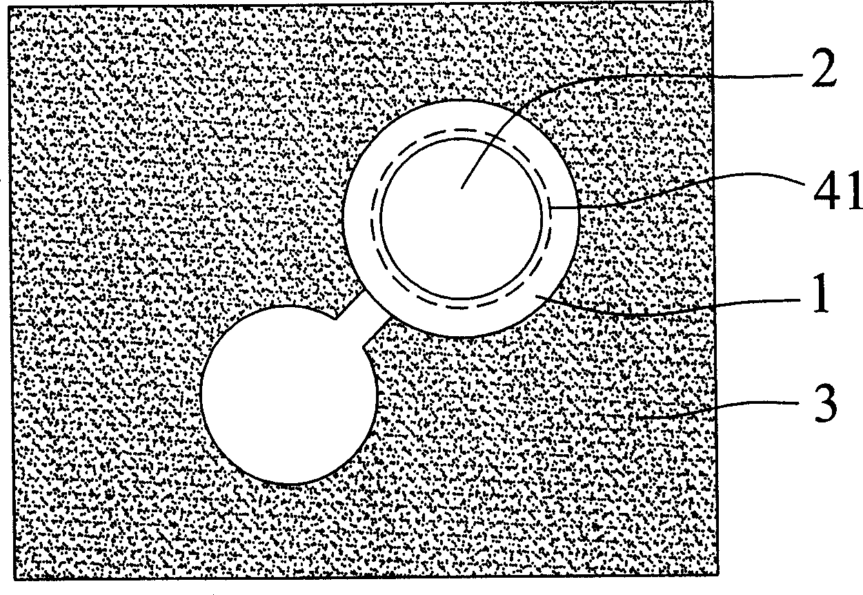
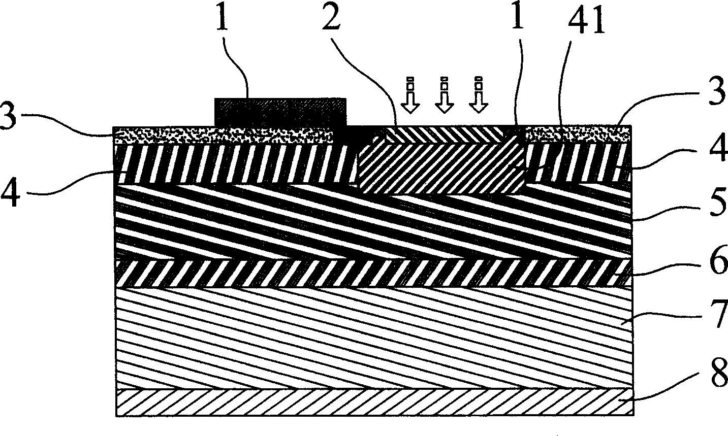
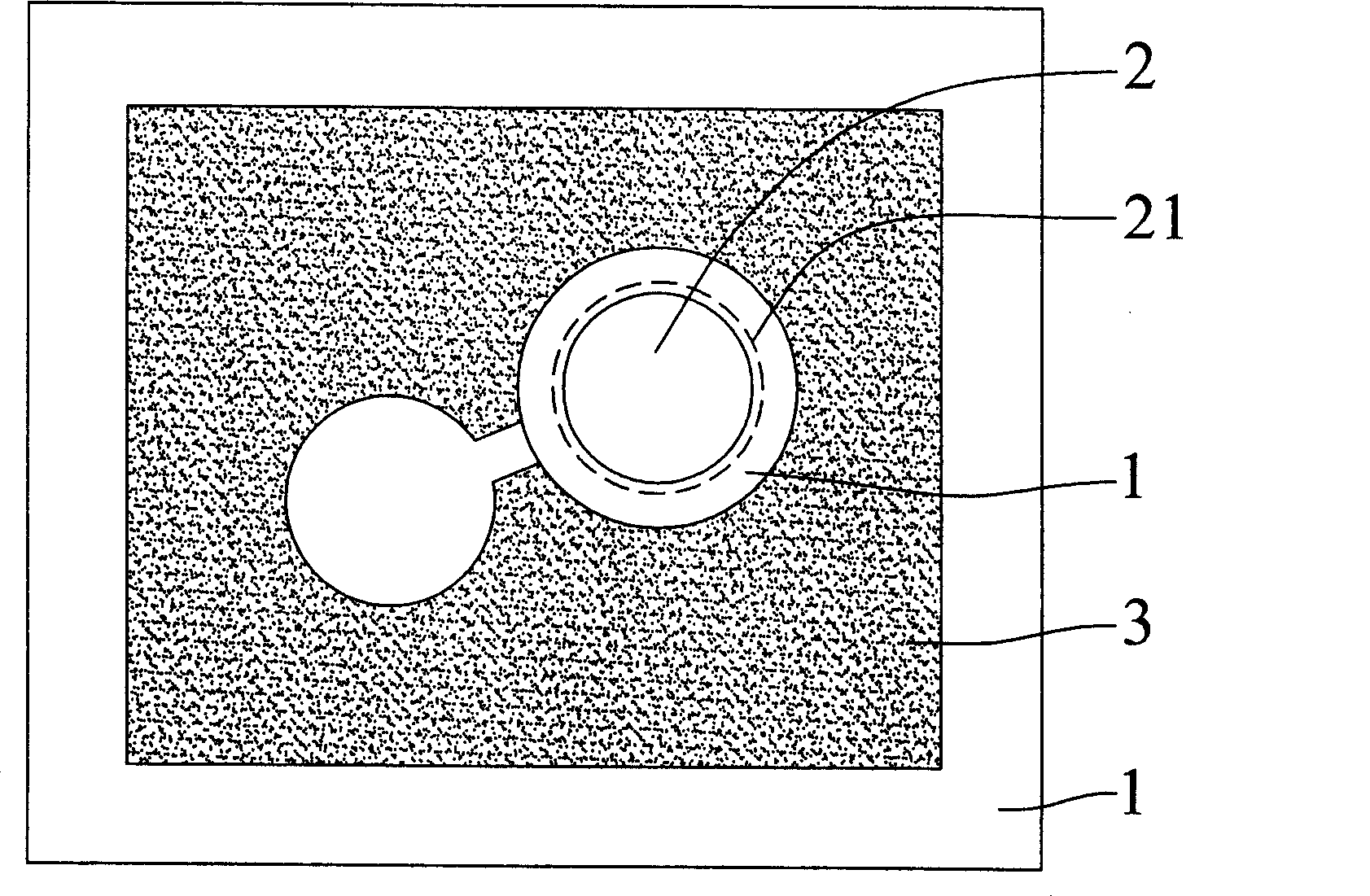
[0014] The atoll-type electrostatic discharge device (refer to image 3 and Figure 4 ), including P-type metal layer 1, light-receiving region 2, resistance-reducing region 21, dielectric layer 3, N - Type semiconductor layer 4, P type semiconductor region 41, i type light absorbing layer 5, N type buffer layer 6, N type substrate 7, N type metal layer 8, be provided with P type metal layer 1 around the photodetector chip, reduce The resistance area 21, the P-type semiconductor area 41, and the atoll-type electrostatic discharge method that cooperates with the chip's ability to resist reverse bias electrostatic damage, so as to avoid damage to the chip due to static electricity, wherein:

[0015] P-type metal layer 1, refers to the reverse bias negative static charge connected to the uppermost metal layer, in the crystal A dumbbell shape is formed in the middle of the surface and the periphery of the chip is formed. The dumbbell shape is formed by connecting two circles. T...


PUM


Abstract

The invention discloses an atoll type electrostatic discharge device for improving the back bias electrostatic damage resistance capability of light tester grains and increasing the electrostatic charge release patches to improve the grain back bias electrostatic damage resistance capability. The electrostatic release paths increased around the light tester grain are a P type metal layer, a resistance reduction area, a P type semiconductor area, an i type light absorption layer, a N type buffering layer, a N type base plate and a N type metal layer. Leading most of the electrostatic charges to release around the grains can avoid most of the electrostatic charges centered among and through the grains and cause grain damage and improve the grain back bias electrostatic damage resistance capability.

Description

technical field [0001] The invention relates to an atoll-type electrostatic discharge device that enhances the ability of a photodetector chip to resist reverse bias electrostatic damage. A P-type metal layer, a resistance-reducing region, and a P-type semiconductor region are arranged around the photodetector chip, and the Most of the static electricity is dispersed and released around the photodetector chip to avoid most of the static electricity concentrated in the middle of the chip, so as to enhance the anti-static damage effect of the chip, and the photodetector chip does not change the process steps , so the manufacturing cost will not be increased, which is in fact fully in line with industrial utilization. Background technique [0002] Press, the chip of conventional photodetector (see figure 1 and figure 2 ), the chip is mainly composed of P-type metal layer 1, light-receiving area 2, dielectric layer 3, N - Type semiconductor layer 4, P-type semiconductor regi...

Claims


Application Information

Patent Timeline
Patent Type & Authority Patents(China)
IPC IPC(8): H01L31/105H01L31/02
Inventor 林蔚
Owner LAND MARK OPTOELECTRONICS
Why Eureka
Try Eureka