Silicon extension of re-doped arsenic substrate

A technology of silicon epitaxy and substrate, which is applied in the direction of electrical components, semiconductor/solid-state device manufacturing, circuits, etc., can solve the problems of high resistance layer of epitaxial layer, affecting impurity content, and the amount of impurity diffusing outward, reaching the transition zone Effects of flatness, suppression of self-doping, and uniform resistivity

Active Publication Date: 2009-01-07
HEBEI POSHING ELECTRONICS TECH
View PDF1 Cites 0 Cited by
  • Summary
  • Abstract
  • Description
  • Claims
  • Application Information

AI Technical Summary

Problems solved by technology

[0015] First of all, in step 1, although HCl corrosion at high temperature can polish the substrate and is beneficial to improve lattice defects, it also has disadvantages: HCl polishing also produces some by-products, and at high temperature When polishing, the surface of the substrate must be peeled off, so even if the large flow of hydrogen is flushed in step 2, some of these by-products and impurities in the substrate will enter the atmosphere of vapor deposition, thus affecting the first step. The impurity content of the intrinsic epitaxial layer, the transition layer
[0016] Second, there is a greater risk of high-resistance interlayers appearing in the intrinsic epitaxial layer grown in the first step
Although the As dopant in the heavily doped As substrate in the first step of growth will diffuse outward to the intrinsic epitaxial layer, and the intrinsic epitaxial layer will be doped with impurities, but due to the edge and middle of the substrate, the impurities outward The amount of diffusion is different, so it is difficult to control, which is very likely to cause a high resistance layer in the intrinsic epitaxial layer, or because the intrinsic epitaxial layer grown in the first step is too thin to completely block the substrate impurities
[0017] In addition, it has been tested through experiments that the resistivity uniformity of the epitaxial layer obtained by the above process can only reach 4% at best, which cannot be further improved; and it is difficult to control the epitaxial uniformity and transition zone of high-resistance thin layers
[0018] Fourth, the above-mentioned "two-step epitaxy" process is effective for preventing vertical self-doping, but not effective for preventing lateral self-doping at the interface

Method used


Image

  • Silicon extension of re-doped arsenic substrate
  • Silicon extension of re-doped arsenic substrate

Examples


Embodiment Construction

[0034] Below in conjunction with concrete experimental result the present invention is described in further detail:

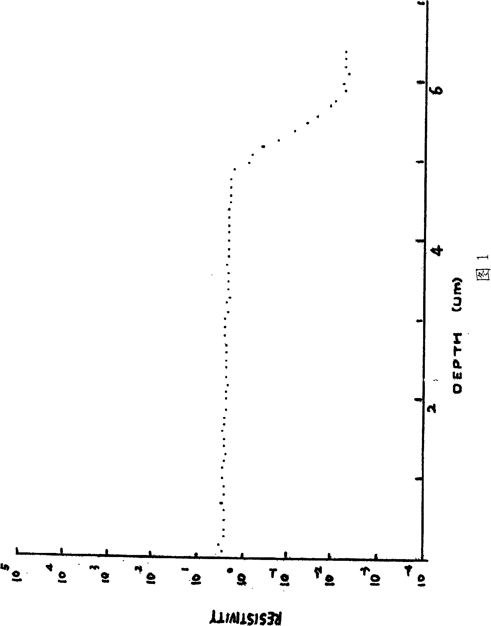
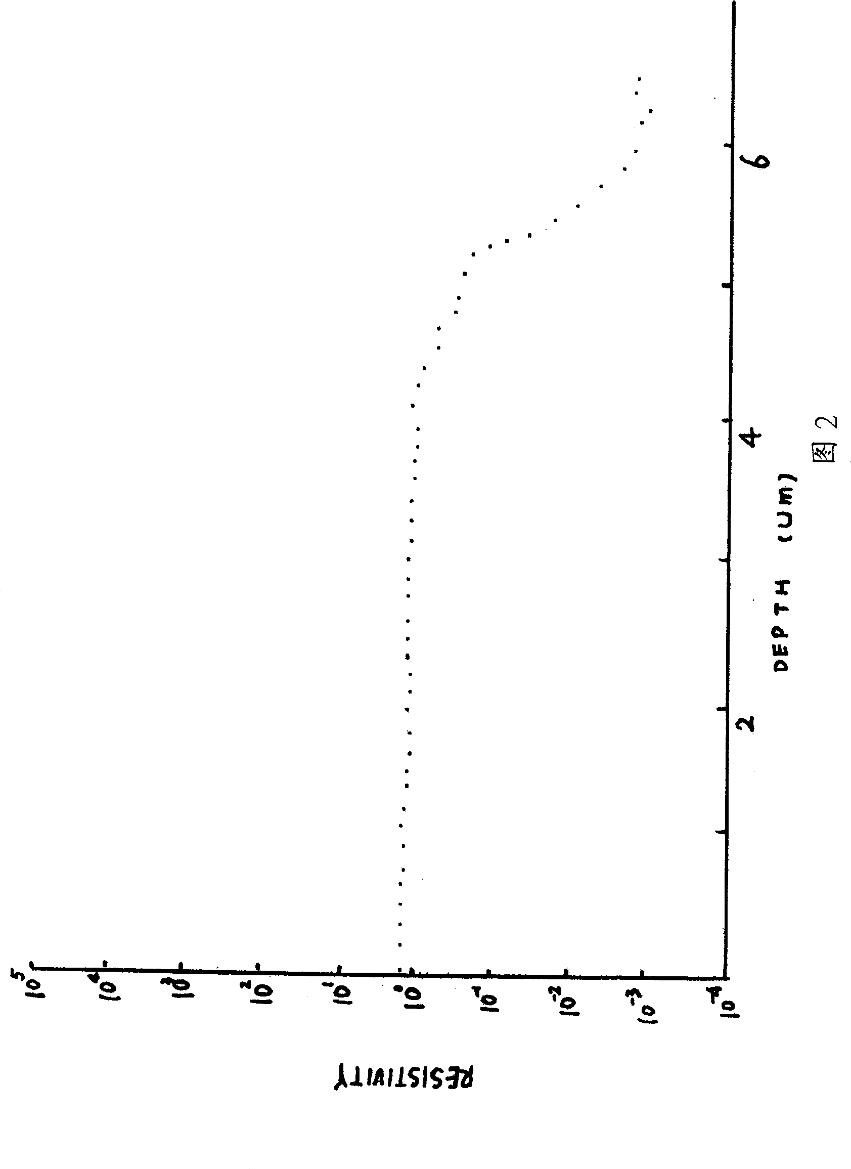
[0035] In this embodiment, the conventional "two-step epitaxy method" and the method of the present invention were used to test respectively, and the test data were compared.

[0036] The epitaxial parameters of the epitaxial layer in this embodiment are: the resistivity of the epitaxial layer is 0.70-0.78Ω·cm, and the thickness of the epitaxial layer is 4.9-5.2um.

[0037] The epitaxial equipment adopted in this embodiment is: PE2061 epitaxial furnace of Italy LPE Company, each furnace can hold 30 four-inch silicon wafers.

[0038] The specific process steps in this embodiment are as follows: Furnace installation-heating to 1000-1200°C-introduction of HCl into the furnace for polishing-use of large flow of H 2 Rinse--grow a layer of intrinsic epitaxial layer with a thickness of about 1.5um--again use large flow H 2 Rinse while passing H 2 Introduce 1% HCl—t...


PUM

PropertyMeasurementUnit
electrical resistivityaaaaaaaaaa

Abstract

The invention is concerned with the manufacture method of the silicon epitaxial slice that is the silicon extension method of remixing arsenic substrate. It is based on the ordinary method, adds the HCI into the flushing H2 when the second time flushing by H2, in order to control autodoping. The smoothness of the resistivity rate and the cragginess of the transition region are all good.

Description

technical field [0001] The invention relates to a method for manufacturing a silicon epitaxial wafer, in particular to a method for manufacturing a heavily arsenic-doped substrate silicon epitaxial wafer by using a hydrogen chloride back-throwing process. Background technique [0002] At present, silicon epitaxial technology on heavily doped arsenic (As) substrate is more and more widely used in the manufacture of electronic devices, and its application scope involves Schottky diodes, triodes, VDMOS, varactor diodes, automotive electronics, IGBTs, etc. In order to improve the die yield, electronic component manufacturers need to strictly control the consistency of the silicon epitaxial wafer on the heavily doped As substrate and the transition region of the epitaxial layer. [0003] In the process of chemical vapor deposition, impurities will inevitably appear in the transition zone of the epitaxial wafer, and the steepness of the impurity distribution in the transition zone...

Claims


Application Information

Patent Timeline
Patent Type & Authority Patents(China)
IPC IPC(8): H01L21/205H01L21/30H01L21/302
Inventor 陈秉克薛宏伟袁肇耿赵丽霞田忠元
Owner HEBEI POSHING ELECTRONICS TECH
Why Eureka
Try Eureka