Fabrication of IGZO oxide TFT on high CTE, low retardation polymer films for LDC-TFT applications

a technology of igzo oxide and high cte, applied in the direction of semiconductor devices, electrical devices, transistors, etc., can solve the problems of low mobility of these devices, inability to adapt to the industry, and inability to manufacture igzo oxide tft on high cte, etc., to achieve high quality

Inactive Publication Date: 2017-08-15
COVESTRO DEUTSCHLAND AG
View PDF26 Cites 3 Cited by
  • Summary
  • Abstract
  • Description
  • Claims
  • Application Information

AI Technical Summary

Benefits of technology

[0005]Accordingly, there exists a need for a high quality TFT on a flexible material which can be produced by an efficient method acceptable for industry applications.

Problems solved by technology

However, the mobilities of these devices are very low and the fabrication methods are not very practical and extensible to industry setup.

Method used


Image

  • Fabrication of IGZO oxide TFT on high CTE, low retardation polymer films for LDC-TFT applications
  • Fabrication of IGZO oxide TFT on high CTE, low retardation polymer films for LDC-TFT applications
  • Fabrication of IGZO oxide TFT on high CTE, low retardation polymer films for LDC-TFT applications

Examples


example 1

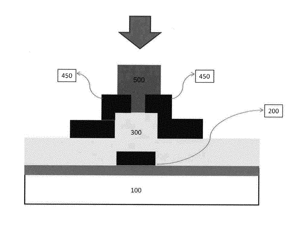
[0103]APEC Polycarbonate (80 μm) coated both sides with a 4 μm high cross linked UV acrylate planarizer (Makrofol® HS279, layer 100, Bayer Material Science AG) sheets were heat treated in Dry Oven (Binder FDL 115) at 180° C. for 72 hours. The film turned slightly yellow. However, pre-annealing in a vacuum oven prevented photo-oxidation and yellowing, and was transparent after 72 hours annealing in vacuum to remove water in the polycarbonate film. Samples of dimensions 35 cm×35 cm were cut.

example 2

[0104]The samples (bottom planarizer coating) obtained in example 1 were laminated onto a glass carrier using a manual roller at room temperature with an Intelimer Tape from Nitta Corporation, (CS2325NA3). For even better lamination, the lamination may be done at 150° C. with an Obducat soft press technology up to 6 MPA (60 bars) so as to achieve a highly optically flat film laminated firmly onto the glass carrier). The samples were then cleaned by sonication in isopropyl alcohol (IPA).

example 3

[0105]An 18 nm coating of aluminum oxide (layer 150) was deposited on top of the planarizer coating of the samples obtained in example 3 by Atomic layer deposition at 150° C. (Savannah 100 from Cambridge Nanotech Inc.) as a water vapour and oxygen barrier as well as an adhesion layer for the aluminum gate.


PUM


Abstract

The present invention provides a TFT on a polymer substrate and a method for producing the TFT. The TFT is, due to its characteristics, particularly suited for applications as backplane in LCD displays and solar cell devices.

Description

CROSS-REFERENCE TO RELATED APPLICATIONS[0001]This application is a national stage application (under 35 U.S.C. §371) of PCT / EP2014 / 070502, filed Sep. 25, 2014, which claims benefit of European Application No. 13186279.9, filed Sep. 27, 2013, both of which are incorporated herein by reference in their entirety.[0002]The present invention relates to a thin film transistor array on a high CTE, low retardation polymer substrate and a method to produce the same. These thin film transistors can be used as TFT backplanes for LCD applications.BACKGROUND OF THE INVENTION[0003]During the past years, the need for organic or thin film transistors (TFT) in industry for use in manufacturing screens of mobile phones, computer and television has increased. Moreover, there is a request for providing TFT on flexible substrates, hence, the replacement of glass by more flexible compounds as substrates. Thus, flexible electronics is a rapidly emerging area with possible applications in displays, sensors...

Claims


Application Information

Patent Timeline
Patent Type & Authority Patents(United States)
IPC IPC(8): H01L29/786H01L29/51H01L29/66H01L29/24H01L21/027H01L21/02H01L29/49H01L29/45H01L29/423H01L27/12
CPCH01L29/7869H01L21/022H01L21/0274H01L21/02118H01L21/02178H01L27/1225H01L27/1259H01L29/24H01L29/42356H01L29/45H01L29/495H01L29/4908H01L29/4958H01L29/4966H01L29/51H01L29/66969H01L29/78603
Inventor OU, ERIC CHUAN WHATTSANKARAN, SIVARAMAKRISHANMA, KHINE MYAT SINTHA.BETA.LER, CHRISTIANSCHMIDT, AXEL
Owner COVESTRO DEUTSCHLAND AG
Why Eureka
Try Eureka