Controlled impedance charged device tester

a technology of impedance charge and device, which is applied in the direction of measuring devices, dielectric strength testing, instruments, etc., can solve the problems of affecting the measurement of discharge current, affecting the test accuracy, and the inability of the protection circuit of the silicon esd protection circuit to turn on sufficiently fast, etc., to achieve the effect of facilitating construction and minimizing reflection

Active Publication Date: 2017-08-08
BARTH JON E
View PDF6 Cites 5 Cited by
  • Summary
  • Abstract
  • Description
  • Claims
  • Application Information

AI Technical Summary

Benefits of technology

The patent describes a design for a gradual impedance transition that minimizes reflections over a wide bandwidth for the duration of the CDM discharge waveform time. This design can be used to simulate the CDM test load impedance and accurately measure the peak current and voltage waveforms of the DUT. The patent also suggests using a constant diameter inner conductor connected to the small diameter pogo pin to contact small pin spacings on an integrated circuit. The optimum impedance transformation ratio for controlled impedance CCDM to simulate the CDM test load impedance is not yet known, so testing a few different values of low impedance transformations can identify the load impedance that will produce the necessary peak current threat that closely simulates that of the CDM test.

Problems solved by technology

This CDM type of ESD event can be fast enough that silicon ESD protection circuits may not turn on sufficiently fast to protect sensitive gate oxides in modern complementary metal-oxide-semiconductor (“CMOS”) circuits.
This will allow some of the ESD voltage to not be fully clamped by the protection circuit, which can damage sensitive gate oxides in the operating part of the IC chip.
Unfortunately, air sparks and metal-to-metal contacts have variable resistances, which cause the measured discharge current to also vary.
This Japanese CCDM method does not control the impedance of the short conductor or the impedance of the switch in the sub nanosecond time frame.
The CDM failure level data does not correlate well with this CCDM test because the high speed impedance of the discharge path is not controlled to simulate the short path CDM discharge impedance.

Method used


Image

  • Controlled impedance charged device tester
  • Controlled impedance charged device tester
  • Controlled impedance charged device tester

Examples


Embodiment Construction

[0027]Reference is now made to the drawings wherein like structures refer to like parts throughout.

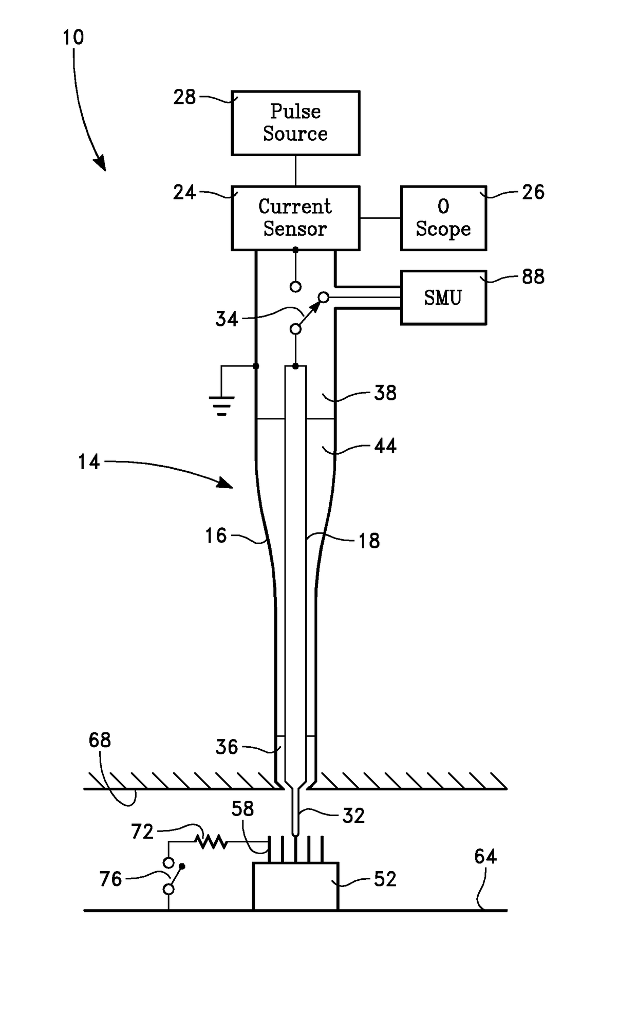
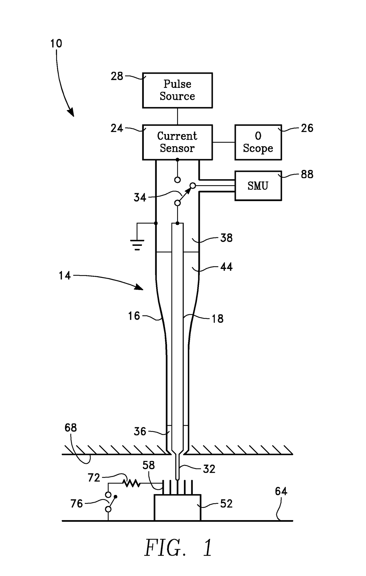
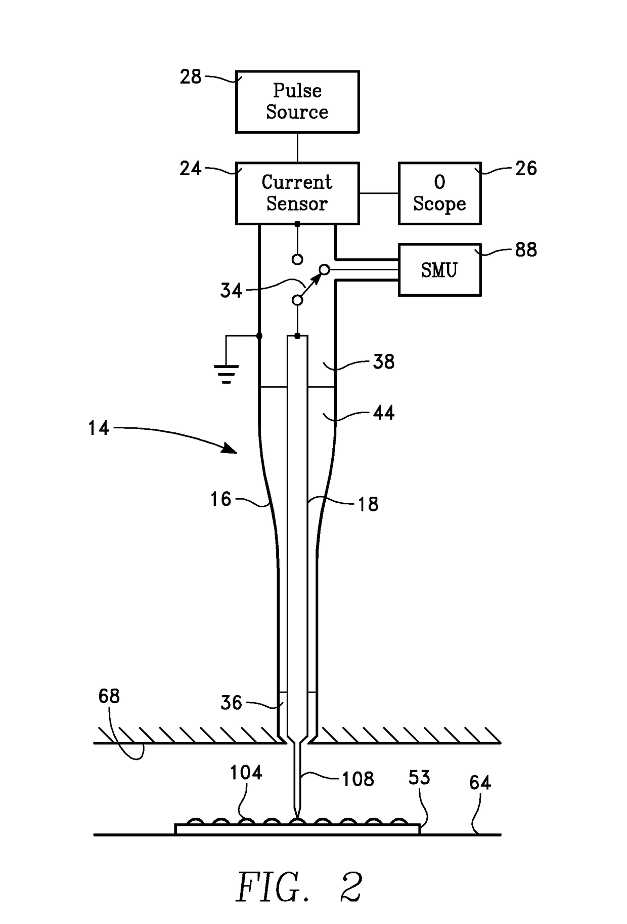
[0028]In FIG. 1, a controlled impedance Charged Device Model (CDM) tester 10 includes a transmission line impedance transformer 14 having an outer conductor 16 and an inner conductor 18. The impedance transformer 14 extends between a 50-ohm high speed coaxial switch (leakage measurement switch) 34 used to connect a DUT 52 to a test pulse source 28. Its DC continuity to the DUT 52 allows a Source Measurement Unit (SMU) 88 to apply a defined test voltage to the DUT lead after each test pulse and measure its DUT leakage current. Silicon DUT failure is identified when the leakage current increases above a limit. When the switch 34 connects the DUT to the pulse source 28 and current sensor 24, the test pulse can be applied to the DUT 52. The current sensor 24 allows the incident waveform to the DUT 52 and the reflected waveform from the DUT 52 to be monitored on an oscilloscope 26.

[0029]The...


PUM


Abstract

An ESD tester transforms high speed pulses from s 50-ohm impedance to the optimum lower impedance necessary to simulate the Charged Device Model (“CDM”) test impedance. Direct connections to the device under test eliminates the variations in spark or contact resistance of the present test while transforming the test pulse impedances to the appropriate level. Direct device connections with controlled impedance current paths provide either internal device discharge or external test pulse testing to simulate the original test. The sparkless direct connection controlled impedance transformation is identified by its ability to simulate similar device failures at similar test voltage failure levels.

Description

RELATED APPLICATIONS[0001]The present application claims the benefit of priority under 35 USC §119 (e) to U.S. Provisional Application No. 61 / 834,255, filed on Jun. 12, 2013, which is incorporated by reference herein for all that it contains.BACKGROUND OF THE INVENTION[0002]Field of the Invention[0003]The present invention relates to an apparatus for Charged Device Model (CDM) testing, which is a specific form of Electro Static Discharge (ESD) testing. More specifically, the present invention relates to a CDM tester utilizing a high speed impedance transformer to control discharge impedance and to transform impedance test pulses of the complete time domain test waveform.[0004]Description of the Related Art[0005]The Charged Device Model (CDM) test was devised to simulate a real world threat when an Integrated Circuit (IC) chip has acquired a charge, such as, for example, the triboelectric charge that builds up a voltage on the IC chip as the chip slides down metal chutes during norma...

Claims


Application Information

Patent Timeline
IPC IPC(8): G01R31/26G01R31/12G01R31/28
CPCG01R31/12G01R31/2855G01R31/002
Inventor BARTH, JON E.
Owner BARTH JON E
Why Eureka
Try Eureka