Double sided Si(Ge)/Sapphire/III-nitride hybrid structure

a hybrid structure and sapphire technology, applied in the field of solid-state physics and semiconductor devices, can solve the problems of reducing thermal conductivity, reducing the c-plane of sapphire not being used for device fabrication, and often showing 90° rotational twin defects

Active Publication Date: 2016-09-20
NASA
View PDF10 Cites 1 Cited by
  • Summary
  • Abstract
  • Description
  • Claims
  • Application Information

AI Technical Summary

Benefits of technology

[0014]One aspect of the present invention is a double sided hybrid crystal structure including a trigonal Sapphire wafer having a (0001) C-plane and having front and rear sides. The Sapphire wafer is substantially transparent to light in the visible and infrared spectra, and also provides insulation with respect to electromagnetic radio frequency noise. The structure includes a layer of crystalline Si material having a cubic diamond structure aligned with the cubic <111> direction on the (0001) C-plane and strained as rhombohedron to thereby enable continuous integration of a selected (SiGe) device onto the rear side of the Sapphire wafer. In some embodiments, the structure includes a layer of crystalline group IV materials comprising one or more of Si, Ge and C and having a cubic diamond structure aligned with the cubic <111> direction on the (0001) C-plane and strained as rhombohedron to thereby enable continuous integration of a selected (SiGe) and / or Si(Ge)(C) device onto the rear side of the Sapphire wafer. The double sided hybrid crystal structure further includes an integrated III-Nitride or ZnO crystalline layer on the front side of the Sapphire wafer that enables continuous integration of a selected III-Nitride or ZnO device onto the front side of the Sapphire wafer.

Problems solved by technology

However, this approach often shows 90° rotated twin defects.
On the other hand, growth of cubic SiGe layers on the trigonal (0001) plane, i.e. C-plane of Sapphire has not been utilized for device fabrication so far due to the formation of 60° rotated twin defects.
While good semiconductor device materials require a single crystalline phase without defects, many good thermoelectric materials have electrically connected poly-type crystalline structures that scatter phonons, thus reducing thermal conductivity.
As also discussed in the Park '368 Patent Application Publication, despite these potential benefits, growing Silicon Germanium in the [111] direction on the trigonally structured C-plane (0001) Sapphire has been a challenge, because this atomic alignment allows poly-type crystalline structures with 60 degree-rotated twin defects as a result of stacking faults as well as twinning on the interface with the underlying trigonal substrate.
Prior attempts to grow single crystalline Si, SiGe, SiGeC on C-Sapphire were generally not successful because it was not known how much single crystal was formed inside the epitaxial material without destroying the sample.

Method used


Image

  • Double sided Si(Ge)/Sapphire/III-nitride hybrid structure
  • Double sided Si(Ge)/Sapphire/III-nitride hybrid structure
  • Double sided Si(Ge)/Sapphire/III-nitride hybrid structure

Examples


Embodiment Construction

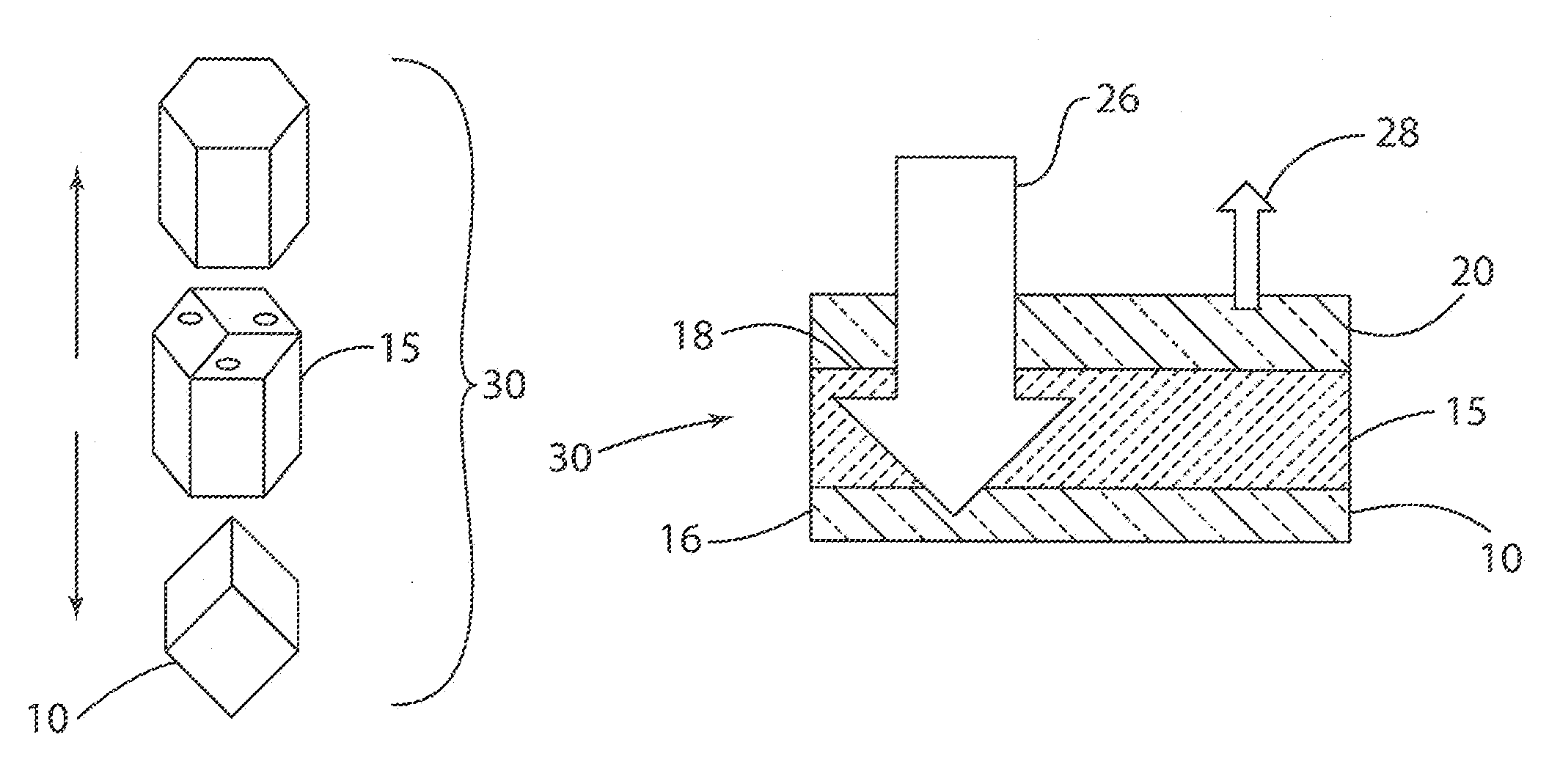
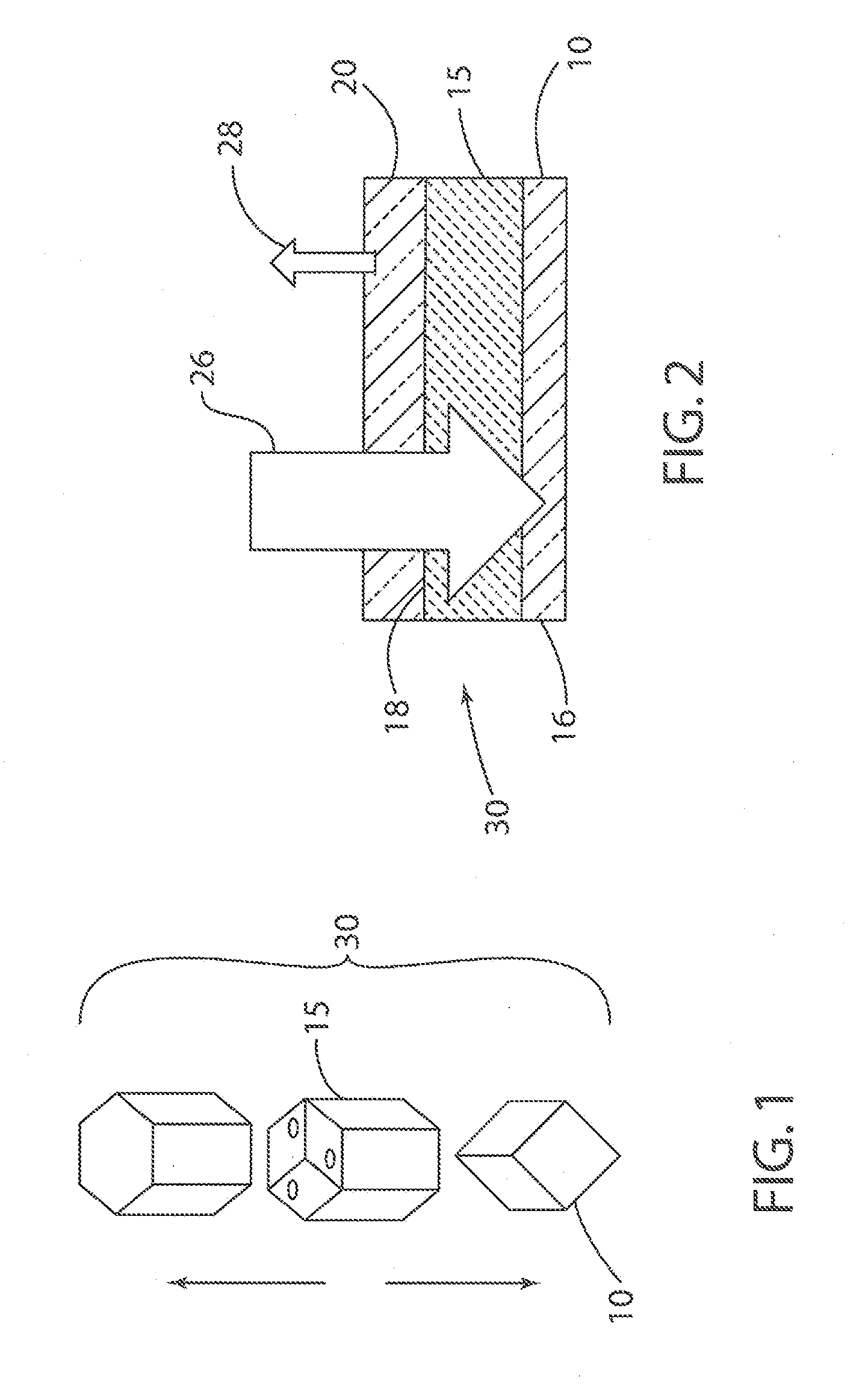
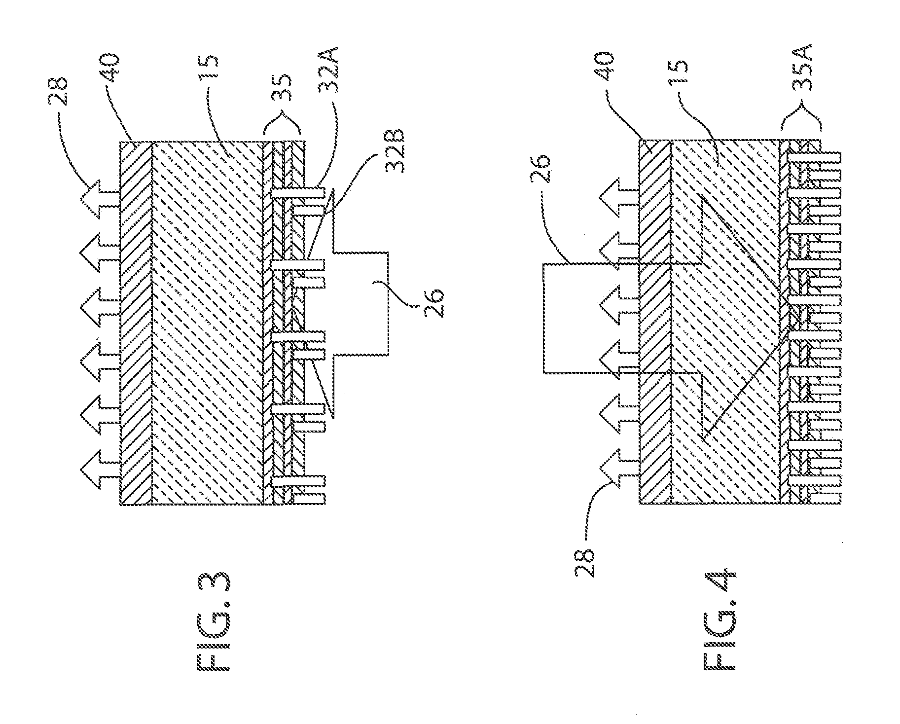
[0022]For purposes of description herein, the terms “upper,”“lower,”“right,”“left,”“rear,”“front,”“vertical,”“horizontal,” and derivatives thereof shall relate to the invention as oriented in FIG. 2. However, it is to be understood that the invention can assume various alternative orientations and step sequences, except where expressly specified to the contrary. It is also to be understood that the specific devices and processes illustrated in the attached drawings, and described in the following specification, are simply exemplary embodiments of the inventive concepts defined in the appended claims. Hence, specific dimensions and other physical characteristics relating to the embodiments disclosed herein are not to be considered as limiting, unless the claims expressly state otherwise.

[0023]Technologies that have recently been developed allow the growth of single crystalline Si and SiGe on C-plane Sapphire. It is described as Rhombohedral super hetero epitaxy because Si and SiGe of...


PUM


Abstract

One aspect of the present invention is a double sided hybrid crystal structure including a trigonal Sapphire wafer containing a (0001) C-plane and having front and rear sides. The Sapphire wafer is substantially transparent to light in the visible and infrared spectra, and also provides insulation with respect to electromagnetic radio frequency noise. A layer of crystalline Si material having a cubic diamond structure aligned with the cubic <111> direction on the (0001) C-plane and strained as rhombohedron to thereby enable continuous integration of a selected (SiGe) device onto the rear side of the Sapphire wafer. The double sided hybrid crystal structure further includes an integrated III-Nitride crystalline layer on the front side of the Sapphire wafer that enables continuous integration of a selected III-Nitride device on the front side of the Sapphire wafer.

Description

CROSS-REFERENCE TO RELATED PATENT APPLICATION(S)[0001]This patent application claims the benefit of and priority to U.S. Provisional Patent Application No. 61 / 783,807, filed on Mar. 14, 2013, the contents of which are hereby incorporated by reference in their entirety.STATEMENT REGARDING FEDERALLY SPONSORED RESEARCH OR DEVELOPMENT[0002]The invention described herein was made in part by employees of the United States Government and may be manufactured and used by or for the Government of the United States of America for governmental purposes without the payment of any royalties thereon or therefore.FIELD OF THE INVENTION[0003]The present invention is in the fields of solid state physics and semiconductor devices, and more specifically to a device including Si / SiGe devices that are grown on the back side of a Sapphire wafer, with III-Nitride devices such as GaN, InGaN, and AIGaN devices on the front side of the Sapphire wafer.BACKGROUND OF THE INVENTION[0004]Various semiconductor devi...

Claims


Application Information

Patent Timeline
Patent Type & Authority Patents(United States)
IPC IPC(8): H01L29/267H01L31/12H01L27/15H01L21/02H01L31/0336H01L31/028H01L31/18H01L31/0368H01L25/16H01L33/00
CPCH01L21/02554H01L21/0242H01L21/0254H01L21/02433H01L21/02532H01L27/15H01L29/267H01L31/028H01L31/0336H01L31/03682H01L31/125H01L31/1804H01L31/1812H01L31/1848H01L31/1852H01L25/167H01L33/007H01L2924/0002Y02E10/544Y02E10/546Y02E10/547Y02P70/521H01L2924/00Y02P70/50H01L21/02529H01L21/2011
Inventor PARK, YEONJOONCHOI, SANG HYOUK
Owner NASA
Why Eureka
Try Eureka