RF device and method with improved active load modulation capability

a technology of active load modulation and rf device, which is applied in the direction of near-field systems using receivers, electrical apparatus, transmission, etc., can solve the problems of unsatisfactory antenna configuration for use in receiving mode, unsatisfactory antenna configuration for use in transmitting mode, etc., and achieve long time for settling voltage at the antenna network, reduce q-factor, increase q-factor

Active Publication Date: 2016-07-26
NXP BV
View PDF12 Cites 10 Cited by
  • Summary
  • Abstract
  • Description
  • Claims
  • Application Information

AI Technical Summary

Benefits of technology

[0007]This aspect is based on the idea that the resonance frequency and the Q-factor of the resonance circuit are optimized to either of the transmission mode and the receiving mode. By choosing the second resonance frequency to be equal to the carrier frequency of a corresponding reader / writer device, a relatively high Q-factor can be obtained such that transmission can take place efficiently. More specifically, the high Q-factor allows greater output power for the side-band levels and thereby a high LMA (load modulation amplitude). Similarly, by choosing a different resonance frequency in the receiving mode, i.e. the first resonance frequency, reception can be optimized as a lower Q-factor provides a greater bandwidth which is beneficial for reception as the received signal is less influenced. Furthermore, this aspect is based on the idea that by periodically modifying the Q-factor of the resonance circuit while the device is in the transmission mode, the long time for settling of the voltages at the antenna network caused by the high Q-factor can be countered. More specifically, by periodically modifying the Q-factor within the modulation pauses during transmission, the antenna circuit is forced back to its idle condition within a short period.
[0022]Thereby, by adjusting the resistance of the adjustable resistive circuit in an alternating manner, the Q-factor of the resonance circuit will alternate between a higher value and a lower value. More specifically, when the resistance of the adjustable resistive circuit is increased, the Q-factor is reduced, and when the resistance of the adjustable resistive circuit is reduced, the Q-factor is increased.
[0023]Accordingly, the above mentioned advantageous effect that the long time for settling of the voltages at the antenna network caused by the high Q-factor can be countered may be obtained in a simple and cost efficient way. In particular, by reducing the Q-factor within the modulation pauses during transmission, the antenna circuit is forced back to its idle condition within a short period.
[0033]The third and fourth aspects of the invention are based on the same idea as the first aspect described in detail above. Furthermore, the third and fourth aspects make it possible to implement the invention in an existing RF device design with only minimum hardware modifications being necessary, i.e. the modification of the resonance circuit.
[0035]Also the fifth aspect is based on the same idea as the first aspect described above. Furthermore, it provides the additional advantage of a matching pair of RF device and reader / writer device.

Problems solved by technology

However, such an antenna configuration is usually not ideal for use in the receiving mode, as the shape of the reader modulation may experience a negative impact.
Similarly, an antenna configuration optimized for the receiving mode is usually not ideal for use in the transmitting mode.

Method used


Image

  • RF device and method with improved active load modulation capability
  • RF device and method with improved active load modulation capability
  • RF device and method with improved active load modulation capability

Examples


Embodiment Construction

[0041]The illustration in the drawing is schematic. It is noted that in different figures, similar or identical elements are provided with the same reference signs or with reference signs, which differ only within the first digit.

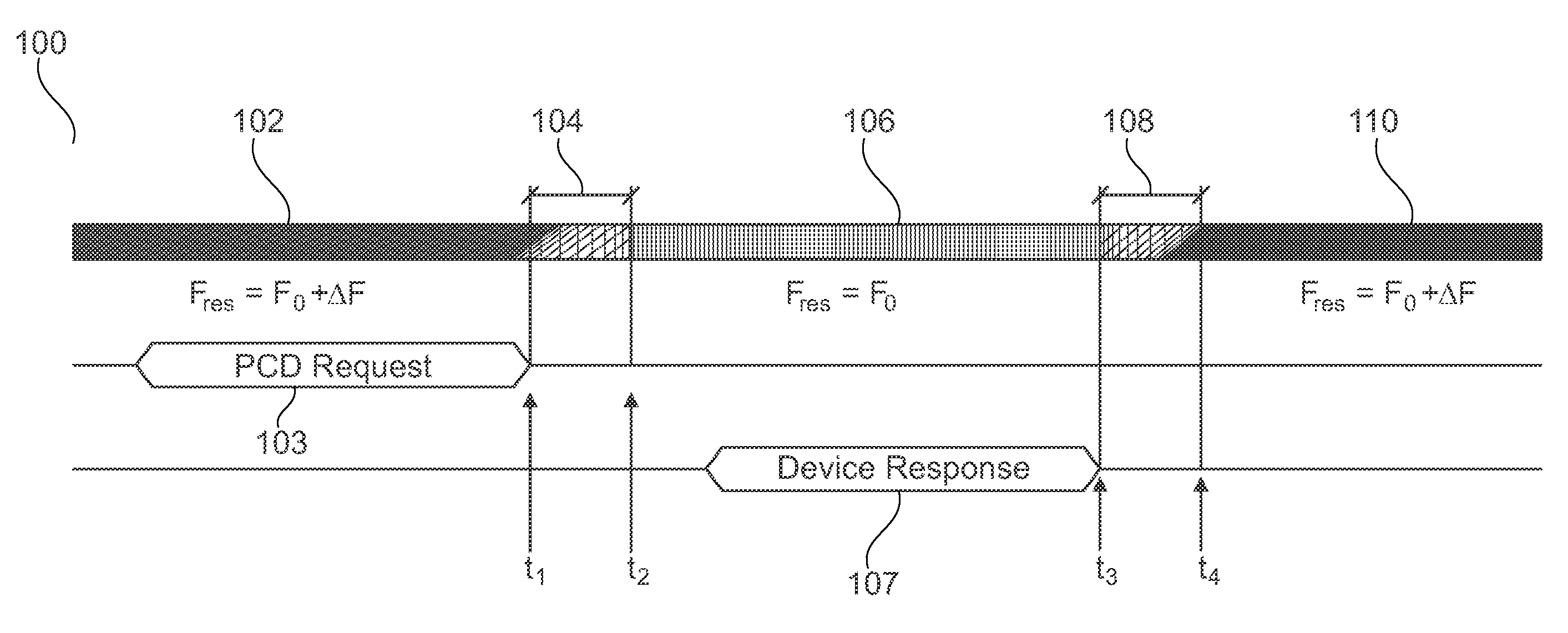
[0042]FIG. 1 shows a schematic overview 100 of bi-directional communication between an RF device and a reader / writer device in accordance with an embodiment. At this stage, the general principle of communication will be discussed. A specific example of a hardware configuration of an RF device is given below in conjunction with FIG. 3.

[0043]More specifically, the left-most part of FIG. 1 shows that an RF device is operating in a receiving mode during period 102. More specifically, the resonance frequency fres of the RF device's resonance circuit is set to f0+Δf, i.e. fres=f0+Δf. Here, f0 is the carrier frequency of a reader / writer device (not shown). During period 102, the RF device receives a request for transmission 103 from the reader / writer device. At ti...


PUM


Abstract

There is described an RF bidirectional communication device utilizing active load modulation, the device comprising (a) a resonance circuit including an antenna (326), and (b) a control unit (322) for controlling communication of the device, including switching between a transmission mode and a receiving mode, wherein the control unit is adapted to (c) modify a configuration of the resonance circuit such that the resonance circuit has a first resonance frequency (f0) when the device is in the transmission mode and a second resonance frequency (f0+Δf) when the device is in the receiving mode, and (d) modify the configuration of the resonance circuit such that a Q-factor of the resonance circuit is periodically decreased while the device is in the transmission mode. There is also described a corresponding method and a system comprising a RF device and a reader / writer device. Furthermore, there is described a computer program and a computer program product.

Description

CROSS-REFERENCE TO RELATED APPLICATIONS[0001]This application claims the priority under 35 U.S.C. §119 of European patent application no. 13177543.9, filed on Jul. 23, 2013, the contents of which are incorporated by reference herein.FIELD OF THE INVENTION[0002]The present invention relates to the field of RF devices, in particular to RF devices for short range or contactless communication using active load modulation.ART BACKGROUND[0003]Recent RF devices, such as contactless transponder cards (e.g. Smartcards, e-Passports, Tickets, etc.) and NFC (Near Field Communication) devices, are capable of performing half-duplex bi-directional communication with a reader device. Thus, these RF devices are capable of operating in a receiving mode as well as in a transmitting mode. In the transmitting mode, RF devices may utilize active load modulation to transmit the information or data. In order to optimize the transmission, the antenna circuit of the RF device is tuned to the carrier frequenc...

Claims


Application Information

Patent Timeline
Patent Type & Authority Patents(United States)
IPC IPC(8): H04B1/44H04B5/00H04B5/02
CPCH04B1/44H04B5/0075H04B5/02
Inventor PIEBER, MICHAELMERLIN, ERICHMENDEL, STEFAN
Owner NXP BV
Why Eureka
Try Eureka