
Symmetric absorber-coupled far-infrared microwave kinetic inductance detector

a far-infrared microwave and kinetic inductance technology, applied in the direction of superconductor details, optical radiation measurement, instruments, etc., can solve the problems of limiting the mkid b, weak crosstalk to the adjacent mkid, and low microwave operating frequency, and achieve the effect of efficient absorption power

Active Publication Date: 2016-07-05
NASA
View PDF1 Cites 10 Cited by
  • Summary
  • Abstract
  • Description
  • Claims
  • Application Information

AI Technical Summary

Benefits of technology

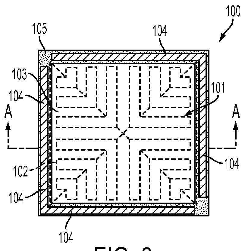
The present invention provides an absorber coupled FIR MKID that can efficiently absorb power at FIR frequencies. It also acts as a half-wave resonator at microwave frequencies and can be used in multiple detector readout systems. The spacing between lines on the membrane is set to minimize reactance and diffractive scattering. The pattern increases the resonance frequency of the detector, allowing for more channels and increased sensitivity. The parallel-plate coupled transmission line minimizes parasitic coupling among adjacent resonator channels.

Problems solved by technology

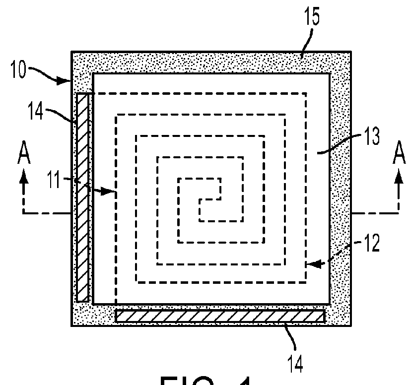
However, disadvantages of the prior art MKID 10 include: 1) a metal pattern 11 which produces asymmetric power coupling for both horizontal and vertical signals; 2) the uniform transmission line used in the resonator results in a high resonator current confined around the center of the microwave kinetic inductance detector (MKID) 10, thus, limiting the MKID 10 sensitivity, and potentially producing strong crosstalk to the adjacent MKID channels; 3) strong parasitic coupling among resonators which produce uncertainty in the resonance frequency calculation, thus, limiting the minimum frequency spacing among MKID channels for large detector array implementations; and 4) the metal pattern 11 on the membrane 13 results in low microwave operating frequencies, which limits the maximum number of resonator channels that can be readout by a cryogenic amplifier.

Method used


Image

  • Symmetric absorber-coupled far-infrared microwave kinetic inductance detector
  • Symmetric absorber-coupled far-infrared microwave kinetic inductance detector
  • Symmetric absorber-coupled far-infrared microwave kinetic inductance detector

Examples


Embodiment Construction

[0046]The present invention relates to an absorber-coupled, extended far-infrared microwave kinetic inductance detector (FIR MKID) array, with cross absorber pattern, which can couple an FIR signal symmetrically at both horizontal and vertical polarizations. The absorber behaves as a half-wave resonator at microwave frequencies and can be used in frequency-multiplexed detector readout systems. The FIR MKID can be readout at higher operating frequencies than conventional MKID designs, thus, increasing the detector array channel capacity. The present invention also produces low parasitic coupling to the adjacent detector channel to simplify the design and minimize interferences.

[0047]In one embodiment, the FIR MKID 100 of the present invention, to which power P is applied (see FIG. 3), is of a suitable size (i.e., 1.03 mm square), and includes a symmetric cross absorber resonator pattern 101 of infrared (IR) absorber 102, disposed on a thin (i.e., approximately 5 μm) membrane 103 of s...


PUM


Abstract

The present invention relates to a symmetric absorber-coupled far-infrared microwave kinetic inductance detector including: a membrane having an absorber disposed thereon in a symmetric cross bar pattern; and a microstrip including a plurality of conductor microstrip lines disposed along all edges of the membrane, and separated from a ground plane by the membrane. The conducting microstrip lines are made from niobium, and the pattern is made from a superconducting material with a transition temperature below niobium, including one of aluminum, titanium nitride, or molybdenum nitride. The pattern is disposed on both a top and a bottom of the membrane, and creates a parallel-plate coupled transmission line on the membrane that acts as a half-wavelength resonator at readout frequencies. The parallel-plate coupled transmission line and the conductor microstrip lines form a stepped impedance resonator. The pattern provides identical power absorption for both horizontal and vertical polarization signals.

Description

ORIGIN OF THE INVENTION[0001]The invention described herein was made by employees of the United States Government and may be manufactured and used by or for the Government for Government purposes without the payment of any royalties thereon or therefore.BACKGROUND OF THE INVENTION[0002]1. Field of the Invention[0003]The present invention relates to an absorber-coupled far-infrared microwave kinetic inductance detector (FIR MKID) array with a symmetric cross pattern which serves dual roles as radiation absorber and superconducting readout. The metal pattern on the inductance detector allows power to be more evenly distributed across the detector area than the prior art, thus, increasing the detector coupling efficiency and sensitivity. Furthermore, the cross absorber pattern allows the output of the detector to readout at more than twice the frequency of a conventional MKID design. Finally, the arrangement of the detector's resonator transmission line minimizes parasitic coupling amo...

Claims


Application Information

Patent Timeline
IPC IPC(8): G01J5/02G01J5/08H01Q1/38H01L39/10H01P7/08G01J1/42
CPCG01J1/42H01P7/082H01L39/10G01J5/046G01J5/20G01J2005/208G01J5/0853G01J5/59H10N60/84
Inventor U-YEN, KONGPOPWOLLACK, EDWARD J.BROWN, ARI D.STEVENSON, THOMAS R.PATEL, AMIL A.
Owner NASA
Learn More