
Method to improve etch selectivity during silicon nitride spacer etch

a technology of silicon nitride and etching, which is applied in the direction of semiconductor devices, electrical equipment, basic electric elements, etc., can solve the problems of difficult to avoid damage or etching the fin, the selectivity requirements are very challenging, and the desired electrical performance cannot be achieved, so as to improve the selectivity of etching and improve the removal of silicon nitride and silicon nitride spacer materials. , the effect of improving the selectivity of etch

Active Publication Date: 2016-04-19
TOKYO ELECTRON LTD
View PDF6 Cites 21 Cited by
  • Summary
  • Abstract
  • Description
  • Claims
  • Application Information

AI Technical Summary

Benefits of technology

The patent describes methods for selectively etching materials on a substrate. By using a cyclical process of etching and oxidation, the techniques described herein can protect silicon surfaces from damage during the etching process. This results in better removal of silicon nitride and silicon nitride spacer materials. Additionally, the patent describes a method that involves a gas flow ratio of halogen-containing gas to oxygen-containing gas that fluctuates between a first gas ratio and a second gas ratio to improve selectivity between SiN and silicon. The technical effects of the patent text include improved selectivity and efficiency in the etching process.

Problems solved by technology

Such partial removal is typically executed using one or more etching processes, but can be challenging because of the differing heights of features being etched simultaneously as well as thicknesses of spacer material.
If not all of the conformal film is removed from around fins then desired electrical performance cannot be achieved.
In a non-planar fabrication scheme, selectivity requirements are very challenging because over-etch amounts or durations needed to clear spacer material from fin-sidewalls are very long compared to etching of planar schemes.
With such long over etch times typically needed, however, it is difficult to avoid damaging or etching the fin.

Method used


Image

  • Method to improve etch selectivity during silicon nitride spacer etch
  • Method to improve etch selectivity during silicon nitride spacer etch
  • Method to improve etch selectivity during silicon nitride spacer etch

Examples


Embodiment Construction

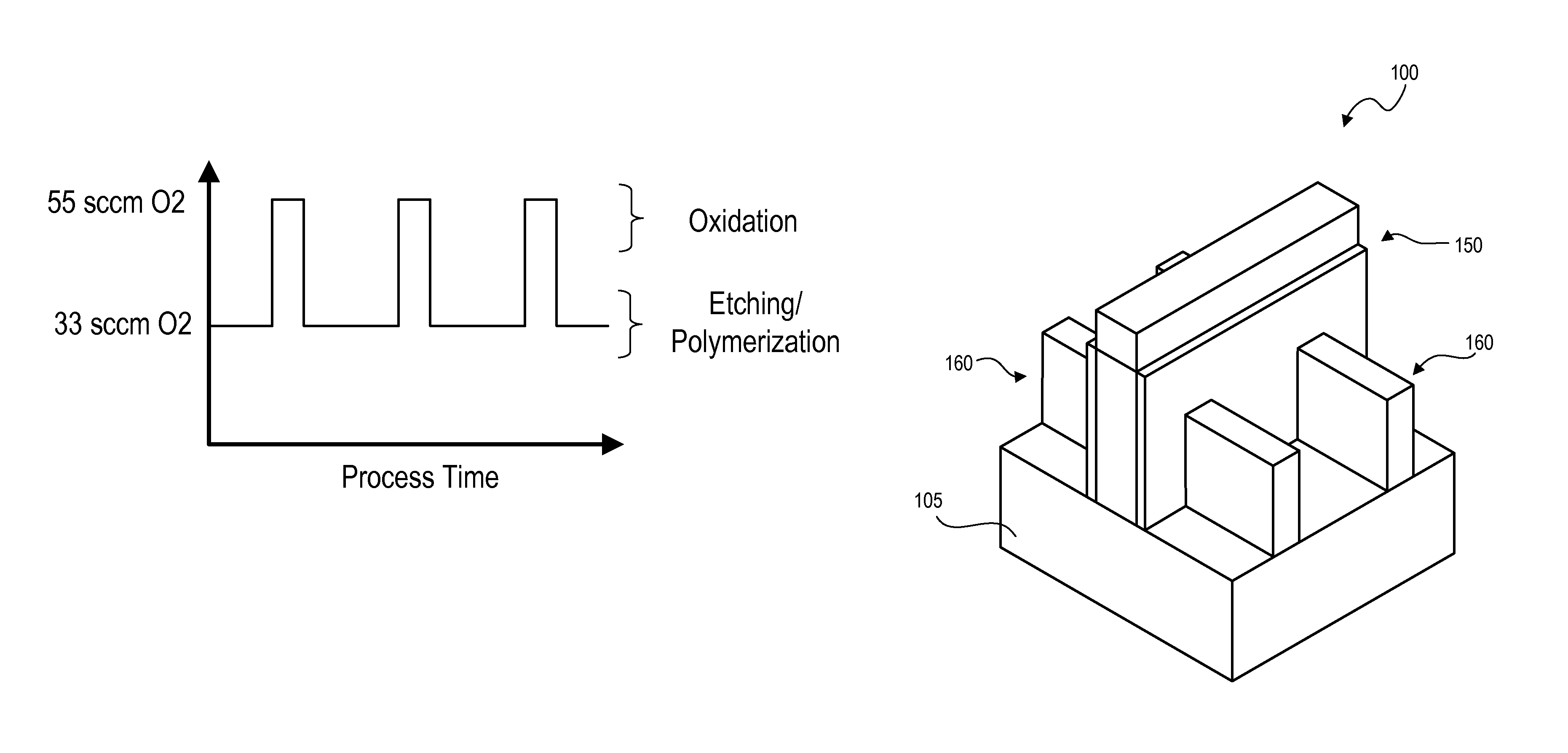
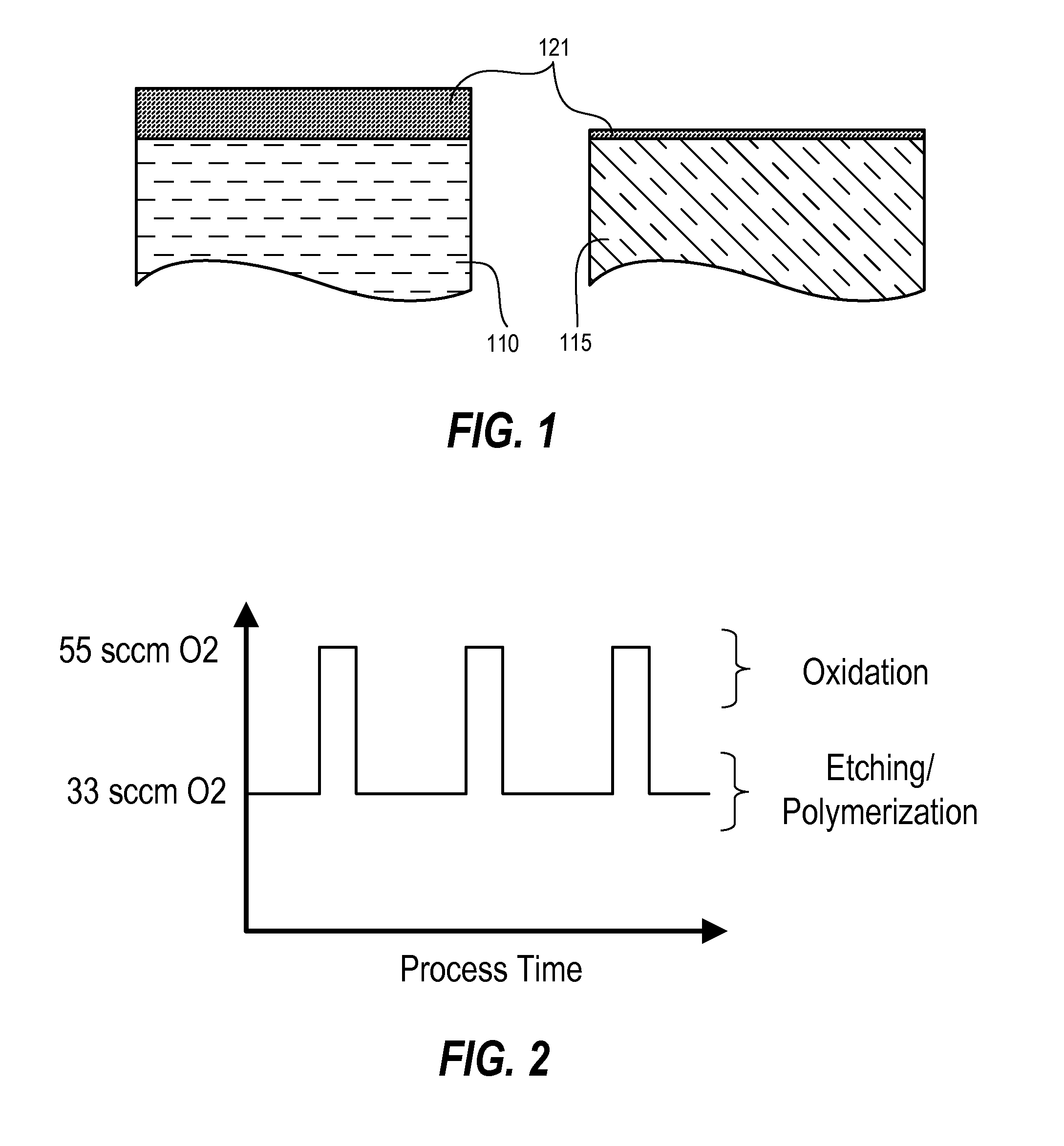
[0020]Techniques herein include methods to increase etching selectivity among materials. Techniques herein include a cyclical process of etching and oxidation of a silicon nitride (SiN) spacer and silicon (such as polycrystalline silicon). This technique can increase selectivity to the silicon so that silicon is less likely to be etched or damaged while silicon nitride is etched from sidewalls and other surfaces. Techniques and chemistries as disclosed herein can be more selective to silicon oxide and silicon as compared to silicon nitride. An oxidizing step creates an oxide protection film on silicon surfaces that is comparatively thicker to any oxide film formed on nitride surfaces. As such, techniques here enable better removal of silicon nitride and silicon nitride spacer materials.

[0021]Improved removal of silicon nitride is enabled in part based on discoveries herein that silicon material (crystalline silicon) oxidizes at a faster and / or thicker rate as compared to oxidation o...


PUM

PropertyMeasurementUnit
etch timeaaaaaaaaaa
etch timeaaaaaaaaaa
etch timeaaaaaaaaaa

Abstract

Techniques herein include methods to increase etching selectivity among materials. Techniques herein include a cyclical process of etching and oxidation of a silicon nitride (SiN) spacer and silicon (such as polycrystalline silicon). This technique can increase selectivity to the silicon so that silicon is less likely to be etched or damaged while silicon nitride is etched from sidewalls. Techniques and chemistries as disclosed herein can be more selective to silicon oxide and silicon as compared to silicon nitride. An oxidizing step creates an oxide protection film on silicon surfaces that is comparatively thicker to any oxide film formed on nitride surfaces. As such, techniques here enable better removal of silicon nitride and silicon nitride spacer materials.

Description

CROSS REFERENCE TO RELATED APPLICATIONS[0001]None.BACKGROUND OF THE INVENTION[0002]This disclosure relates to fabrication of features in a semiconductor device, including fabrication via etching and deposition processes.[0003]Fabrication of semiconductor devices is a multi-step process of forming features on a semiconductor substrate or other substrate. Steps can include material growth, patterning, doping, deposition, etching, metallization, planarization, and so forth. Features formed on a substrate can include various transistors. Transistors can be planar or non-planar, and can also have single gates or multiple gates. Non-planar transistors (sometimes referred to as 3D transistors) include the FinFET (fin field effect transistor), among others. Such non-planar transistors typically include a vertically-oriented or raised fin that functions as a channel between the source and drain. The gate is also vertically-oriented or raised and is positioned over the fin (on top of the fin ...

Claims


Application Information

Patent Timeline
Patent Type & Authority Patents(United States)
IPC IPC(8): H01L21/461H01L21/311H01L29/66H01L29/51H01L21/02H01L21/318
CPCH01L21/31116H01L21/02337H01L29/518H01L29/6656H01L29/66795H01L21/3185
Inventor RANJAN, ALOKPARKINSON, BLAKE
Owner TOKYO ELECTRON LTD
Learn More