Ordering structure of scintillator and fabrication method

a technology of order structure and scintillator, which is applied in the direction of instruments, x/gamma/cosmic radiation measurement, liquid/solution decomposition chemical coating, etc., can solve the problems of reducing the efficiency of csi scintillators, high manufacturing time and cost of csi scintillators, and emitted effectively, etc., to achieve low cost, rapid production, and low manufacturing processing time

Active Publication Date: 2016-04-19
NAT CHUNG SHAN INST SCI & TECH
View PDF7 Cites 4 Cited by
  • Summary
  • Abstract
  • Description
  • Claims
  • Application Information

AI Technical Summary

Benefits of technology

The present invention provides a scintillator with sub-micron column structure that can be manufactured by anodic treatment and die casting technology with low cost and rapid production. The scintillator has advantages of low manufacture-processing time, low cost and simple manufacturing process. Additionally, the invention also provides a method for manufacturing the scintillator with sub-micron column structure, through which the scintillator can be made by anodic treatment and die casting technology with low cost and rapid production. The film oxidized metal tubes of the tubular template can be further manufactured to nano tubes with adjustable membrane size, thickness, and vessel density. Overall, the invention provides a cost-effective, efficient method for producing scintillators with sub-micron column structure.

Problems solved by technology

Since crystalline scintillator includes high energy gap, the photons still cannot be effectively emitted although large electrons in conduction band migrate to valence band, or, the emitted photons cannot become visible light due to there high energy.
On the other hand, traditional CsI scintillator process would cause some drawbacks in the CsI scintillator, for example, yellow discolouration, air pores, cloudiness, etc., and the yellow discolouration, the air pores and the cloudiness would impact the output of visible light and further reduce the efficiency of the CsI scintillator.
However, the mask, lithography, exposure, etching, and crystal growth equipments adopted in semiconductor process technology result in high manufacturing time and cost to CsI scintillator.

Method used


Image

  • Ordering structure of scintillator and fabrication method
  • Ordering structure of scintillator and fabrication method
  • Ordering structure of scintillator and fabrication method

Examples


Embodiment Construction

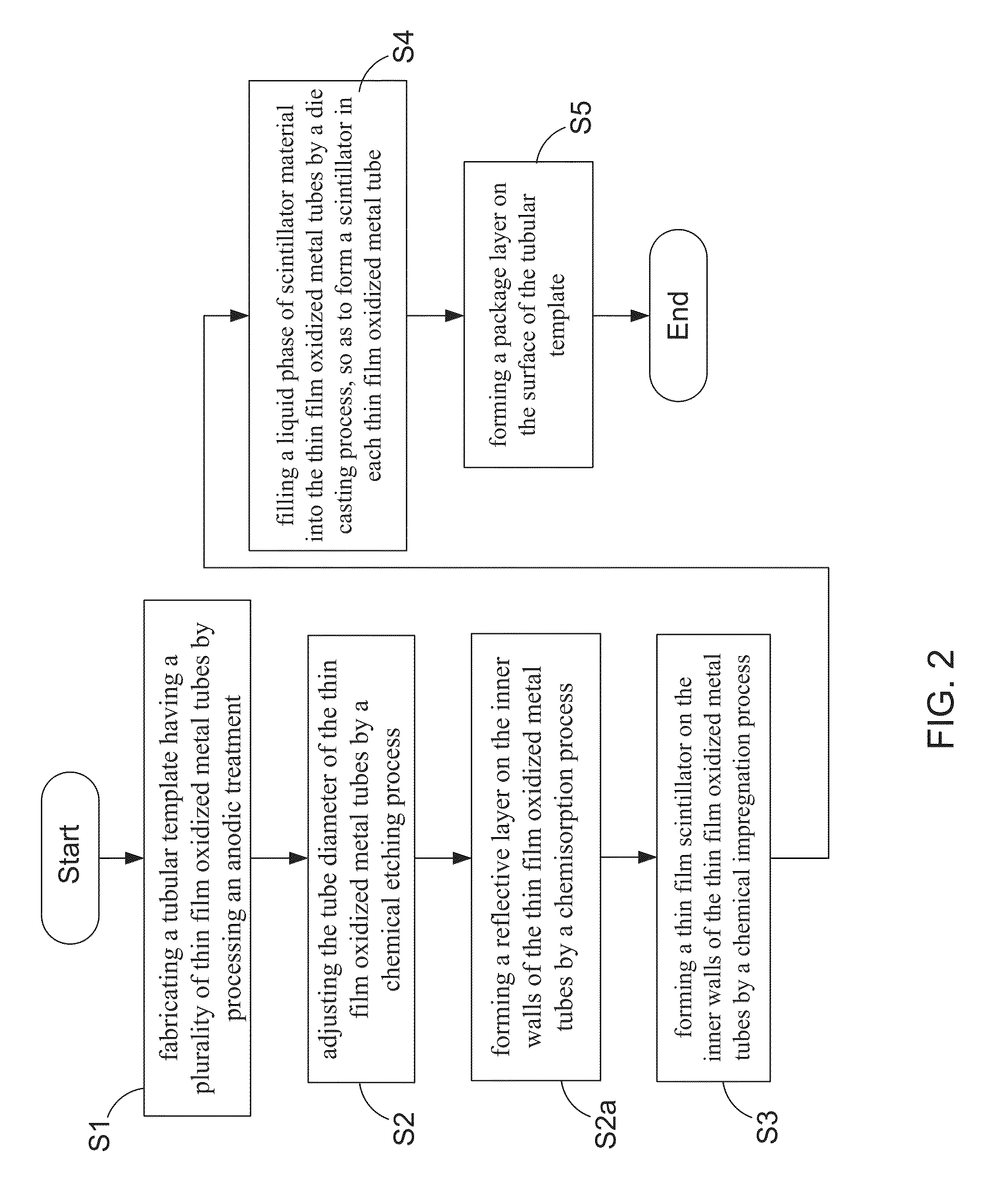
[0044]To more clearly describe a scintillator with sub-micron column structure and a manufacturing method thereof according to the present invention, embodiments of the present invention will be described in detail with reference to the attached drawings hereinafter.

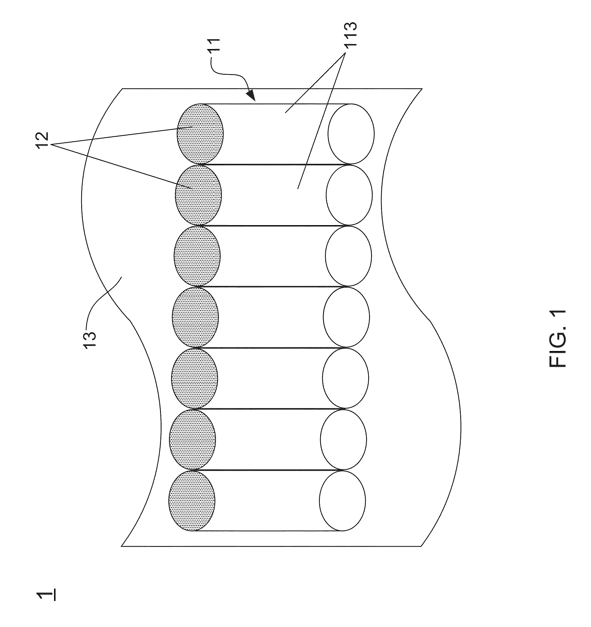
[0045]Please refer to FIG. 1, which illustrates a framework view of a scintillator with sub-micron column structure according to the present invention. As shown in FIG. 1, the scintillator with sub-micron column structure 1 mainly includes a tubular template 11, a plurality of scintillators 12 and a package layer 13, wherein the tubular template 11 consists of a plurality of thin film oxidized metal tubes 113, the scintillators 12 are respectively filled in the thin film oxidized metal tubes 113, and the package layer 13 is formed on the surface of the tubular template 11 for protecting the scintillators 12 from being damaged by water vapor and oxygen. In the present invention, the package layer 13 can be a polymer, a me...


PUM

PropertyMeasurementUnit
specific tube diameteraaaaaaaaaa
timeaaaaaaaaaa

Abstract

An ordering structure scintillator of scintillator and fabrication method is disclosed. The ordering structure scintillator of scintillator comprises: a tubular template, which consists of a plurality of thin film oxidized metal tubes; a plurality of scintillators, filled in the thin film oxidized metal tubes; and a package layer, formed on the surface of the tubular template for protecting the tubular template. In addition, through the fabrication method, the ordering structure scintillator of scintillator can be made by anodic treatment and die casting technology with low cost and rapid production; moreover, the film oxidized metal tubes of the tubular template can be further manufactured to nano tubes by adjusting electrolyte composition, electrolysis voltage, and processing time of anodic treatment, and the aperture size, the thickness and the vessel density of the nano tube can be controlled and ranged from 10 nm to 500 nm, 0.1 μm to 1000 μm, and 108 to 1012 tube / cm2, respectively.

Description

BACKGROUND OF THE INVENTION[0001]1. Technical Field[0002]The present invention relates to a scintillator structure and a manufacturing method thereof, and more particularly, to a scintillator with sub-micron column structure and a manufacturing method for making the same, wherein the manufacturing method is used for making the scintillator with sub-micron column structure, and the scintillator with sub-micron column structure is able to transform the X-ray to a visible light for being applied in medical equipments, nuclear medicine, and security detection technologies.[0003]2. Description of Related Art[0004]Scintillator is a product of high-energy physics technology, which is used for transforming X-ray to an electronic signal or a visible light; therefore, the visible light transformed from X-ray can be further converted to an electronic signal by conventional optics device, for example, charge-coupled device (CCD). The scintillation occurring in the scintillator is a fluorescence...

Claims


Application Information

Patent Timeline
Patent Type & Authority Patents(United States)
IPC IPC(8): G01T1/20C23C18/36C23G1/12G01T1/202G01T1/00C25F3/20C25D11/26C25D11/24C25D11/16C25D11/12C25D11/08C25D11/04C23C18/16C25D1/02B44C1/22C23C18/18
CPCG01T1/003B44C1/227C23C18/1616C23C18/1879C23C18/36C23G1/125C25D1/02C25D11/045C25D11/08C25D11/12C25D11/16C25D11/24C25D11/26C25F3/20G01T1/202G01T1/2006
Inventor CHEN, CHIEN-CHON
Owner NAT CHUNG SHAN INST SCI & TECH
Why Eureka
Try Eureka