Charged particle beam microscope
a particle beam microscope and microscope technology, applied in the field of charged particle beam microscopes, can solve the problems of shrinkage, volume shrinkage, and the original dimension of the pattern cannot be measured correctly, and achieve the effect of not lowering the throughput of pattern dimension measuremen
- Summary
- Abstract
- Description
- Claims
- Application Information
AI Technical Summary
Benefits of technology
Problems solved by technology
Method used
Image
Examples
first embodiment
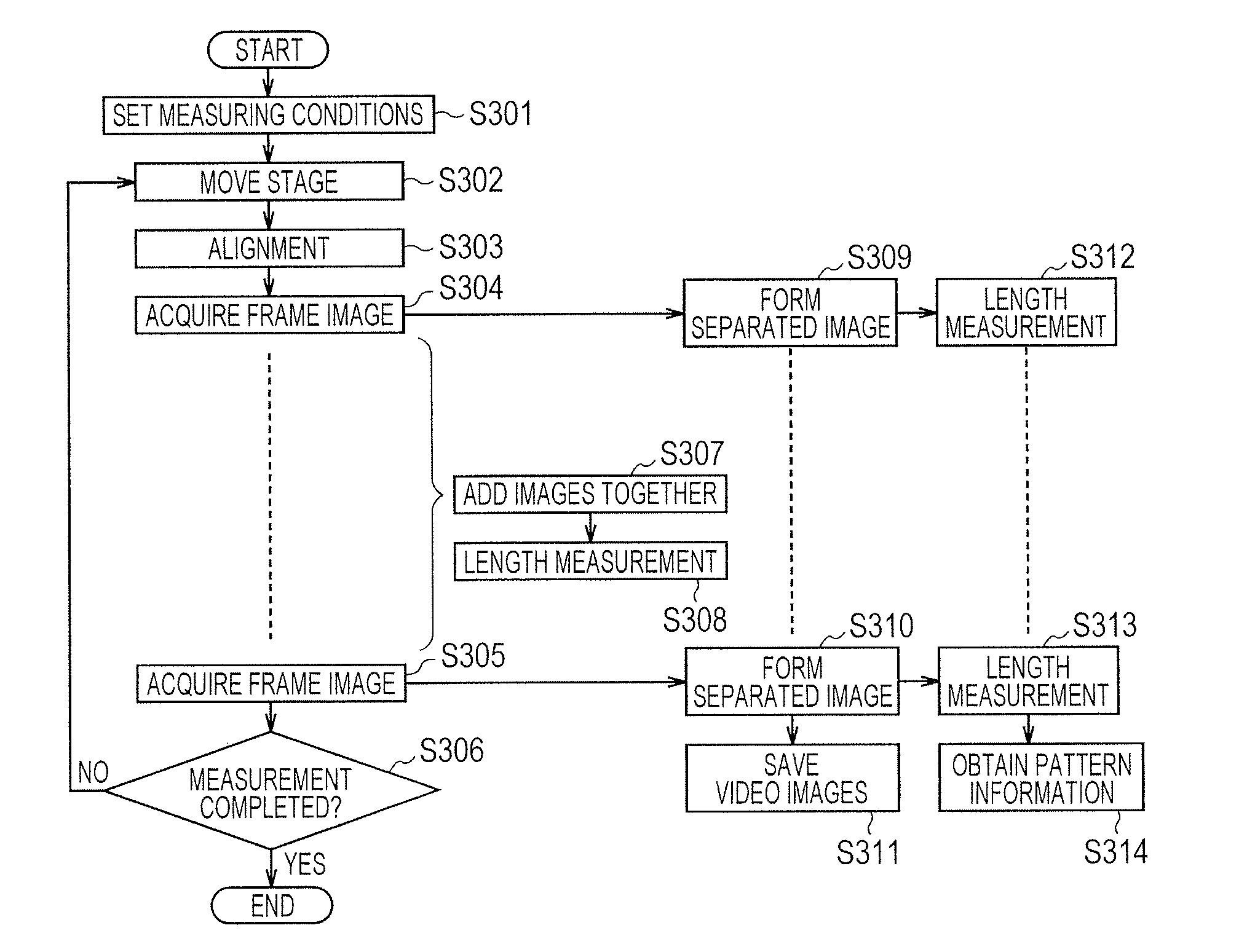
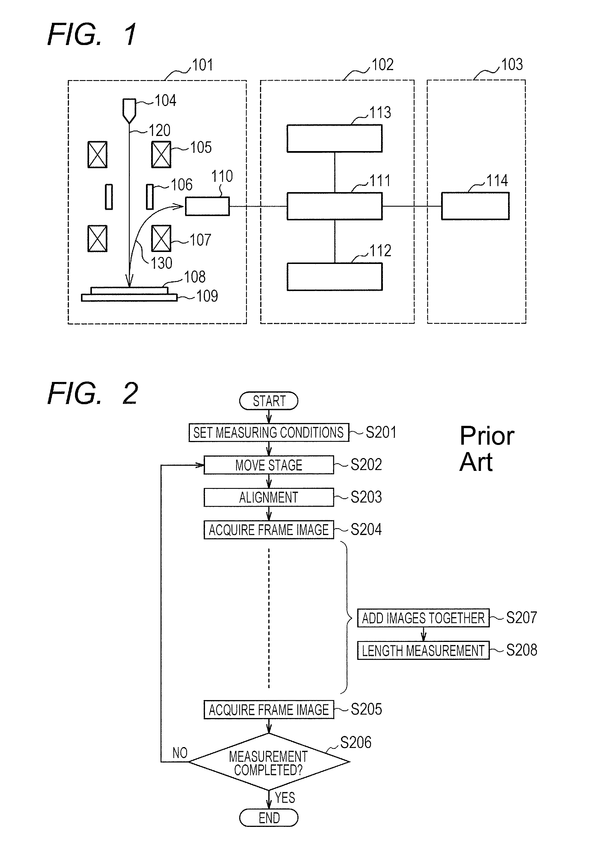
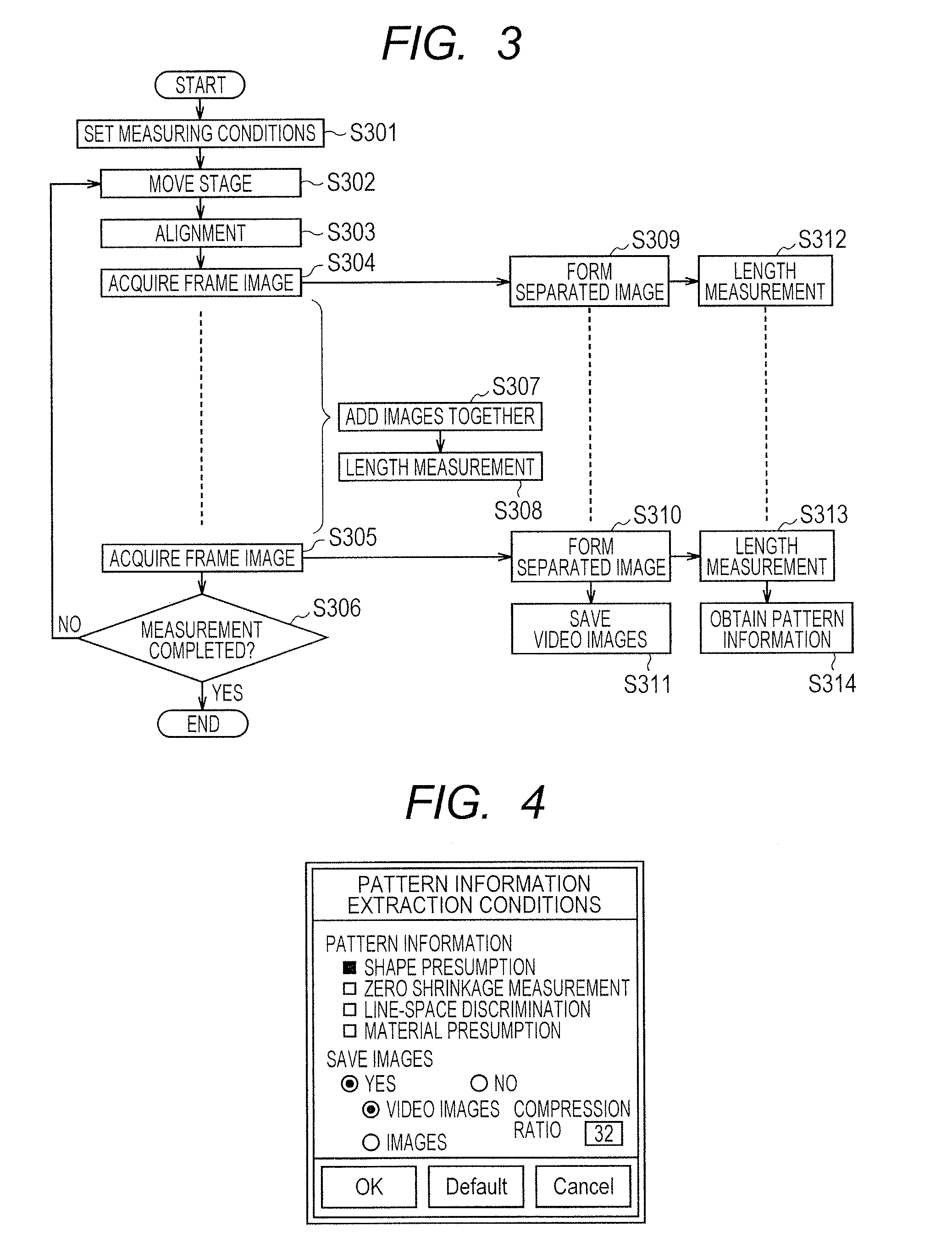
[0037]A first embodiment will be described referring to FIG. 1 to FIG. 8. FIG. 1 is a view showing the configuration of a scanning electron microscope according to this embodiment. This device has a function to make an image for length measurement by adding together frame images and measure lengths and makes it possible to obtain pattern information from change over time of plural frame images constituting the image for length measurement. Here, an image made by adding together plural frame images acquired by scanning the field of view once is defined as an image for length measurement.
[0038]The scanning electron microscope with a function to obtain pattern information includes an electron microscope unit 101, a control unit 102, and a display unit 103. An electron beam 120 emitted from an electron source 104 is converged by a condenser lens 105 and an objective lens 107 and then thrown on a sample 108 placed on a sample stage 109. The electron beam is scanned over the sample two-di...
second embodiment
[0068]A second embodiment will be described referring to FIG. 9 and FIG. 10. What has been described about the first embodiment is also applicable to this embodiment unless there are special circumstances. In this embodiment, zero shrinkage presumption will be explained.
[0069]FIG. 9 show a method of measuring dimensions before shrinkage by comparison with the conventional method. FIG. 9A shows the conventional method of calculating zero time values and FIG. 9B shows the method according to the present invention.
[0070]First, FIG. 9A is explained. The process of acquiring an image for length measurement by scanning the spot to be observed more than once is first carried out more than once and the length measurement value of each image for length measurement is calculated. The length measurement value is plotted on the vertical axis versus the number of measurements on the horizontal axis. Since the resist pattern tends to have a characteristic that it shrinks due to electron beam irra...
third embodiment
[0082]A third embodiment will be described referring to FIG. 12 and FIG. 13. What has been described about the first embodiment is also applicable to this embodiment unless there are special circumstances. In this embodiment, an explanation is given of a technique of deciding whether for a resist pattern it is a pattern to remain intact (Line pattern) or a portion to be lost (Space pattern).
[0083]FIG. 12A shows an example of an image of a pattern being observed. Shown here is an example that no difference in shading contrast is seen between the Line portions and Space portions. Not only in this case, this technique can be applied in a case that shading is seen but discrimination between patterns to remain intact and portions to be lost is impossible or a case that the shading contrast of a pattern changes during observation. In order to address this problem, in this embodiment, length measurement values of neighboring pattern widths CD1 and CD2 are measured.
[0084]FIG. 12B shows the ...
PUM
 Abstract
Description
Claims
Application Information
 - R&D
- Intellectual Property
- Life Sciences
- Materials
- Tech Scout
- Unparalleled Data Quality
- Higher Quality Content
- 60% Fewer Hallucinations
Browse by: Latest US Patents, China's latest patents, Technical Efficacy Thesaurus, Application Domain, Technology Topic, Popular Technical Reports.
© 2025 PatSnap. All rights reserved.Legal|Privacy policy|Modern Slavery Act Transparency Statement|Sitemap|About US| Contact US: help@patsnap.com


