
Organic semiconductor polymer, composition for organic semiconductor material, and photovoltaic cell

a semiconductor and organic technology, applied in semiconductor devices, photovoltaic energy generation, solid-state devices, etc., can solve the problems of insufficient insufficient durability of polymers, and insufficient photoelectric conversion efficiency of organic thin-film solar cells, etc., to achieve excellent durability, less uneven film thickness, and excellent photoelectric conversion efficiency

Active Publication Date: 2016-01-26
FUJIFILM CORP
View PDF18 Cites 0 Cited by
  • Summary
  • Abstract
  • Description
  • Claims
  • Application Information

AI Technical Summary

Benefits of technology

The present invention provides an organic semiconductor polymer with excellent photoelectric conversion efficiency and durability, especially in the presence of oxygen. The polymer has uniform battery performance even at different locations in the photoelectric conversion layer. A composition for organic semiconductor materials is also provided, as well as a photovoltaic cell (especially an organic thin film solar cell) that includes the polymer or composition. A polymer can also be provided.

Problems solved by technology

However, the photoelectric conversion efficiency of organic thin film solar cells is still insufficient.
However, in both cases, the conversion efficiency of the solar cell using the above-mentioned polymers is not necessarily sufficient, and these polymers are not satisfactory in terms of durability, and particularly in terms of durability in the presence of oxygen.

Method used


Image

  • Organic semiconductor polymer, composition for organic semiconductor material, and photovoltaic cell
  • Organic semiconductor polymer, composition for organic semiconductor material, and photovoltaic cell
  • Organic semiconductor polymer, composition for organic semiconductor material, and photovoltaic cell

Examples


examples

[0166]The present invention will be described in more detail based on the following examples. The materials, used amounts, proportions, treatments, treatment procedures and the like indicated in the following Examples can be appropriately modified as long as the purport of the present invention is maintained. It is therefore understood that the present invention is by no means intended to be limited to the specific examples below.

experiment 1

Synthesis of Polymer 1

[0167]Synthesis was carried out as shown in Scheme 1 described below.

[0168]

(Synthesis of Intermediate 2)

[0169]111.3 g of Compound 1 and 38.1 g of thiourea were added to 250 ml of ethanol, and the mixture was heated to reflux for 2 hours. The reaction liquid was poured into ice water, and a 10% aqueous solution of sodium hydroxide was added thereto until the reaction liquid turned weakly alkaline. The mixture was extracted with ethyl acetate. The extract was washed with a saturated aqueous solution of sodium hydrogen carbonate and saturated brine, and then was dried over anhydrous magnesium sulfate. After filtration, the solvent was distilled off under reduced pressure, and the residue was crystallized from an ethyl acetate / hexane mixed solvent. Thus, 100.2 g of an intermediate 2 was obtained. Yield: 82.0%.

(Synthesis of Intermediate 3)

[0170]56.5 g of copper (II) chloride was added to 1 L of acetonitrile, and 44.5 g of isoamyl nitrite was added thereto at room te...

experiment 2

Synthesis of Polymer 2

[0183]Synthesis was carried out as shown in Scheme 2 described below. An intermediate 14 was synthesized by the same technique as in Experiment 1.

[0184]

(Synthesis of Polymer 2)

[0185]In a nitrogen atmosphere, 60.0 mg of magnesium fragments were introduced into 50 ml of dry THF, and a solution prepared by dissolving 91.9 mg of the intermediate 14 in 10 ml of dry THF was slowly added dropwise thereto. While the state in which fine foaming from magnesium was sustained was maintained, dropwise addition of the solution of the intermediate 14 was continued. After completion of the dropwise addition, the mixture was further stirred for one hour at 50° C. The mixture was left to cool naturally, and then this solution was taken out with a syringe and was added to a suspension prepared by dispersing 50 mg of (1,3-bis(diphenylphosphino)propane)nickel chloride in 20 ml of dry THF. This mixture was heated to 50° C., and was allowed to react for 10 hours. After the reaction ...


PUM

PropertyMeasurementUnit
wavelengthsaaaaaaaaaa
HOMOaaaaaaaaaa
energy levelaaaaaaaaaa

Abstract

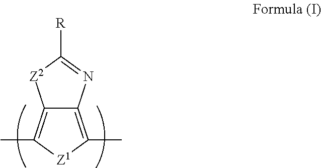
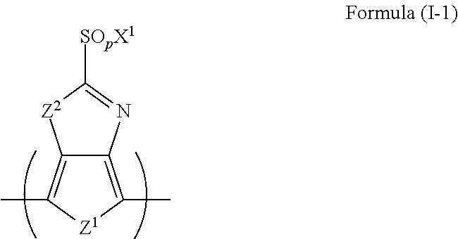
An organic semiconductor polymer comprising a structural unit represented by the following Formula (I), a composition for organic semiconductor material, a photovoltaic cell and a polymer.wherein Z1 and Z2 each independently represent S, O, Se or Te; R represents —SOpX, —CN, —NO2, —P(═O)(OR1,)(OR2) or —C(R1′)═C(CN)2; X represents a hydrogen atom, an alkyl group, a cycloalkyl group, an aryl group, an aromatic heterocyclic group or —NR3(R4); R1, R2, R1,, R3 and R4 each independently represent a hydrogen atom, an alkyl group, a cycloalkyl group, an aryl group or an aromatic heterocyclic group; R3 and R4 may bond with each other to form a ring; and p represents 1 or 2.

Description

TECHNICAL FIELD[0001]The present invention relates to an organic semiconductor polymer, a composition for organic semiconductor material and a photovoltaic cell.BACKGROUND ART[0002]Organic semiconductor polymers have been a subject of active research in recent years in the field of organic electronics, and the polymers are used in organic electroluminescent elements that emit light when electricity is passed, organic photoelectric conversion elements that generate power when irradiated with light, organic thin film transistor elements that control the amount of current or the amount of voltage, and the like. In such an element, similarly to an inorganic semiconductor material, use is made of an organic semiconductor material obtained by combining a p-type conductive semiconductor material, which is an electron donor material, and an n-type conductive semiconductor material, which is an electron acceptor material.[0003]In recent years, since fossil energy of petroleum and the like em...

Claims


Application Information

Patent Timeline
Patent Type & Authority Patents(United States)
IPC IPC(8): H01L31/00C08G61/12H01L51/00H01L51/42H10K99/00
CPCH01L51/0043C08G61/123C08G61/126H01L51/0036C08G2261/124C08G2261/145C08G2261/1452C08G2261/3241C08G2261/3243C08G2261/3246C08G2261/414C08G2261/91H01L51/0037H01L51/4253Y02E10/549H10K85/1135H10K85/113H10K30/30H10K30/50H10K85/151
Inventor NAKAI, YOSHIHIROSUGIURA, HIROKITAKEUCHI, KIYOSHI
Owner FUJIFILM CORP
Learn More