
Thermal detectors using graphene and oxides of graphene and methods of making the same

a technology of graphene oxides and detectors, applied in the direction of optical radiation measurement, instruments, semiconductor devices, etc., can solve the problems of affecting and most photodetectors disadvantageously not integrated with existing microelectronics technology, etc., to achieve the elimination of nyquist limited behavior and improve the performance of ir detection systems

Active Publication Date: 2015-11-24
MAGNOLIA OPTICAL TECH
View PDF24 Cites 42 Cited by
  • Summary
  • Abstract
  • Description
  • Claims
  • Application Information

AI Technical Summary

Benefits of technology

The invention removes a limitation on the detection of IR light called Nyquist frequency limitation, which is caused by the presence of certain types of noise. This limitation is overcome because graphene nanoribbons exhibit no measurable noise sources of these types. Optical systems with fl have significantly improved performance as a result.

Problems solved by technology

Besides silicon, most photodetectors disadvantageously do not integrate with existing microelectronics technology, usually detect only a specific wavelength (i.e. 1.1 mm for Si, 0.87 mm for GaAs, 0.414 mm for a-SiC and 1.89 mm for Ge), and require multiple detectors to detect a broad band of wavelengths (hence photon energy).
Bolometers operate by absorbing radiation, which in turn raises the temperature of the material and hence alters the resistance of the material.
Since bolometers detect a broad range of radiation above a few microns, bolometers are typically thermally stabilized to reduce the possibility of detection of blackbody radiation that is emitted from the detector material, which leads to a high background noise.
This performance is limited by 1 / f noise and the basic physical properties of the vanadium oxide film.

Method used


Image

  • Thermal detectors using graphene and oxides of graphene and methods of making the same
  • Thermal detectors using graphene and oxides of graphene and methods of making the same
  • Thermal detectors using graphene and oxides of graphene and methods of making the same

Examples


Embodiment Construction

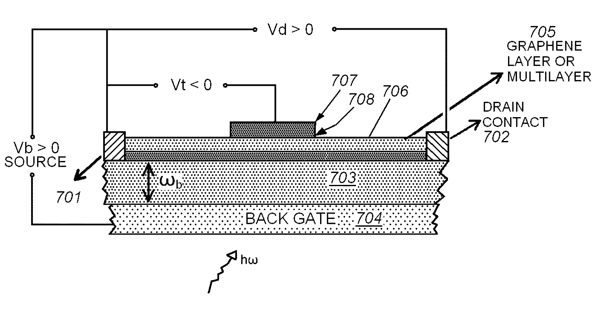
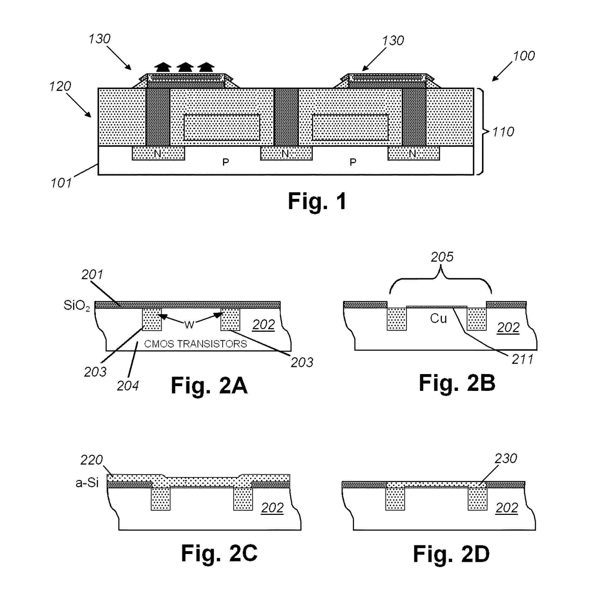
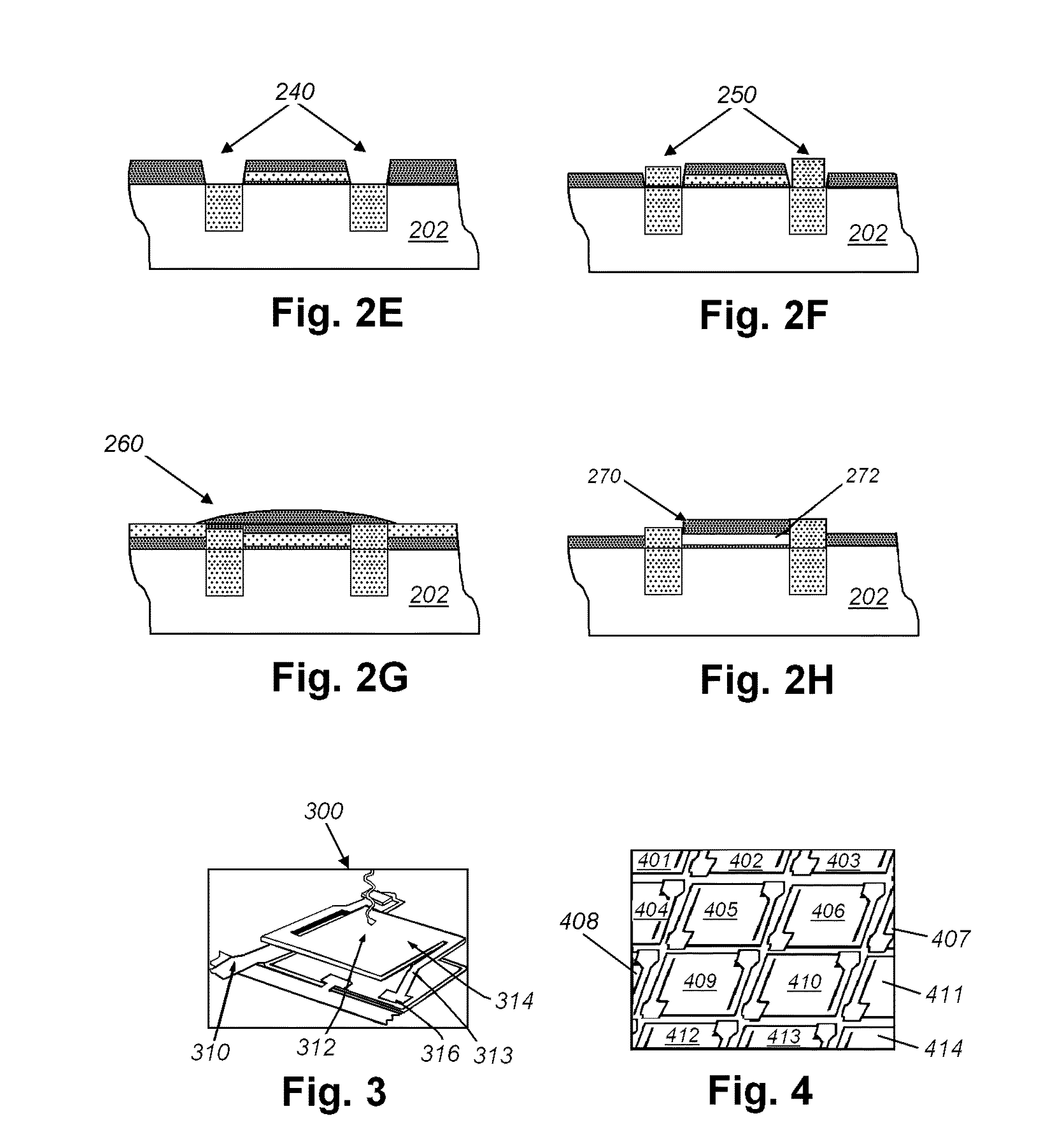
[0033]Devices including graphene single layers or multilayers suspended over gaps (for example, gaps of approximately 50-250 nm) can be employed as Infrared (IR) radiation detectors. In addition, the application of graphene single layer or multilayers on a thermally isolated cantilever beam can be employed as an IR radiation detector.

[0034]Graphene based detectors have several important and unique features that are not available with existing technologies. First, arrays of these nanotube light detectors can be formed using patterning technology at minimum dimensions of the lithography node used or dictated by the demands of the optical imaging system. It is possible to create 25, 17, or 8 micron square or less detectors limited only by photolithography techniques.

[0035]Illustrative embodiments of the invention allow integration at a level of one light detector per ten or less transistors at the minimum dimension of a given lithography node or the integration of large arrays that are...


PUM


Abstract

Radiation detecting and sensing systems using graphene and methods of making the same are provided; including a substrate, a single or multiple layers of graphene nanoribbons, first and second conducting interconnects each in electrical communication with the graphene layers. Graphene layers are tuned to increase the temperature coefficient of resistance, increasing sensitivity to IR radiation. Absorption over a wide wavelength range (200 nm to 1 mm) is possible based on the three alternative devices structures described within. Devices can variously include (a) a microbolometer based graphene film where the TCR of the layer is enhanced with selected functionalization molecules, (b) graphene layers with a source and drain metal interconnect and a deposited metal of SiO2 gate which modulates the current flow across the phototransistor detector, and / or (c) tuned graphene layers layered on top of each other where a p-type layer and a n-type layer is created using a combination of oxidation and doping.

Description

RELATED APPLICATIONS[0001]This application claims the benefit of U.S. Provisional Application Ser. No. 61 / 638,243, filed Apr. 25, 2012, entitled THERMAL DETECTORS USING GRAPHENE AND OXIDES OF GRAPHENE AND METHODS OF MAKING THE SAME, the entire disclosure of which is herein incorporated by reference.FIELD OF THE INVENTION[0002]The present application relates generally to bundled nanotube fabrics and methods of making graphene for use in Ultraviolet (UV), Infrared (IR) and Terahertz radiation detecting and sensing systems.BACKGROUND OF THE INVENTION[0003]Photodetectors are an integral part of optical circuits and components (for example emitters, modulators, repeaters, waveguides or fibers, reflectors, resonators, detectors, IR Focal plane arrays, UV microchannel arrays and THZ diode detectors etc.) and are used for the sensing of electromagnetic radiation. There are several approaches to these devices. Photoconducting materials, typically semiconductors, have electrical properties th...

Claims


Application Information

Patent Timeline
IPC IPC(8): H01L29/06H01L31/00H01L31/028
CPCH01L31/028G01J5/20H01L29/1606H01L31/08H01L31/112G01J5/046G01J5/22G01J5/24G01J5/0853Y02E10/547H01L31/101
Inventor EGERTON, ELWOOD J.SOOD, ASHOK K.
Owner MAGNOLIA OPTICAL TECH
Learn More