Flash-to-ROM conversion

a flash-to-rom and conversion technology, applied in the direction of read-only memories, instruments, static storage, etc., can solve the problems of expensive flash-to-rom conversion, and inability to achieve large-scaled down arrays

Active Publication Date: 2015-04-07
TOWER SEMICONDUCTOR
View PDF9 Cites 3 Cited by
  • Summary
  • Abstract
  • Description
  • Claims
  • Application Information

AI Technical Summary

Benefits of technology

[0012]In accordance with a first embodiment, an S-Flash memory cell is converted to a ROM cell (hereinafter an “S-ROM cell”) by introducing a threshold voltage implant into the channel region of the S-Flash memory cell to cause the resulting S-ROM cell to have a relatively high threshold voltage (i.e., store a first logic state), or preventing the threshold voltage implant from being introduced into the channel region of the S-Flash memory cell to cause the resulting S-ROM cell to have a relatively low threshold voltage (i.e., store a second logic state).
[0013]In accordance with a second embodiment, an S-Flash memory cell is converted to an S-ROM cell by introducing a threshold voltage implant into a substrate region in alignment with an edge of the gate electrode of the S-Flash memory cell. The threshold voltage implant region extends under the gate electrode, and also extends under a charge storage structure formed at the sidewall of the gate electrode. The threshold voltage implant region increases the threshold voltage of a reverse read operation performed in the S-ROM cell, thereby indicating a first logic state. The threshold voltage implant region is prevented from being introduced into the substrate region to indicate a second logic state.
[0014]In accordance with a third embodiment, the width of the mask through which the threshold voltage implant of the second embodiment is performed is varied, thereby allowing the threshold voltage implant region to have different dopant concentrations, thereby allowing multiple bits to be represented by the S-ROM cell.

Problems solved by technology

It usually takes a significant amount of time to implement a Flash-to-ROM conversion because the Flash memory technologies and ROM technologies are different.
Consequently, the Flash-to-ROM conversion is expensive and time consuming.
Conventional attempts to perform a Flash-to-ROM conversion with minimum changes to the embedded Flash cells and array organization have been somewhat successful only for arrays that implement Flash cells that include both select transistors and storage transistors (i.e., cells having two transistors), and therefore feature rather large cells, thus making the idea impractical for large scaled down arrays.
Each ROM element includes a select transistor and a ROM transistor, so the layout of these cells is undesirably large.
However, Weiner does not facilitate a Flash-to-ROM process, because the expensive EEPROM technology is still used to form the ROM elements.
However, the memory cell proposed by Hsu is only suitable for memory units that include select transistors (i.e., two (or more) transistors per memory unit).
In addition, there is no option to change the programmed OTP code, thus making conversion to ROM process complicated.
Both Eitan and Yang undesirably require a complicated NROM-like technology that requires special masks for patterning the bit lines, and also requires special oxides and special etch procedures.
NROM technology and array organization (bit lines orthogonal to polysilicon word lines) is not attractive for Flash-to-ROM conversion because many additional masks and process steps are needed, and the array periphery (i.e., read-out circuits) must be changed to implement the Flash-to-ROM conversion.

Method used


Image

  • Flash-to-ROM conversion
  • Flash-to-ROM conversion
  • Flash-to-ROM conversion

Examples


first embodiment

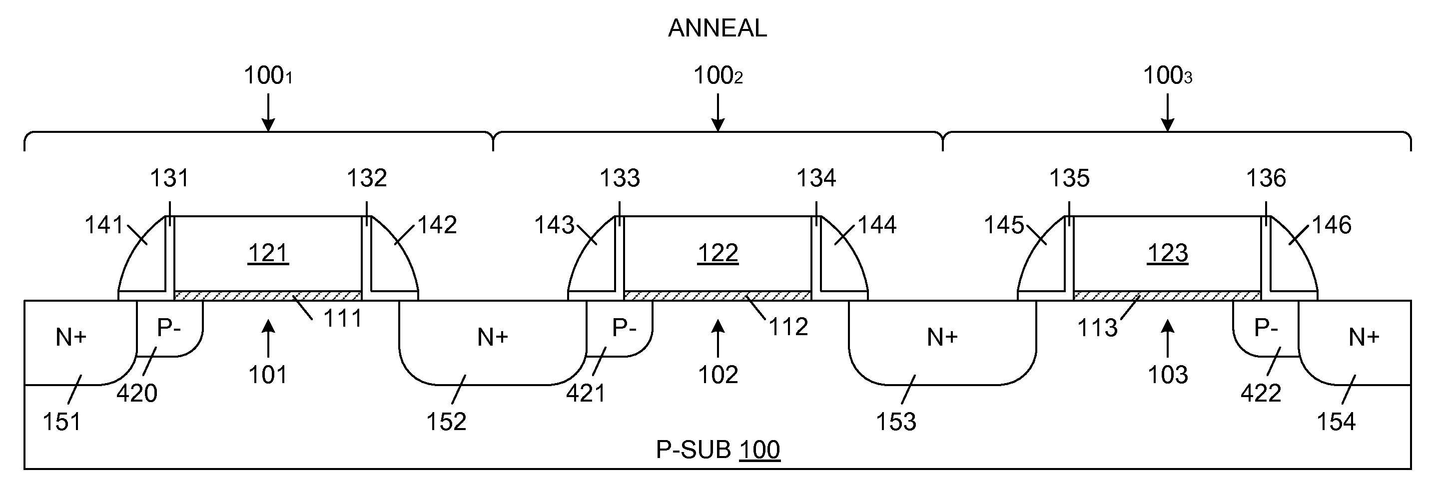
[0031]In accordance with a first embodiment of the present invention, a Flash-to-ROM conversion is implemented by modifying a method used to fabricate S-flash memory cell array 200. In general, a threshold voltage (VT) implant is introduced into the channel regions of S-flash cells that are to have a first logic state (i.e., are ‘programmed’ to have a high threshold voltage) as a result of the Flash-to-ROM conversion, while the threshold voltage implant is prevented from entering the channel regions of S-flash cells that are to have a second logic state (i.e., have a low threshold voltage) as a result of the Flash-to-ROM conversion.

[0032]FIGS. 3A-3F are cross sectional views that illustrate a Flash-to-ROM conversion of S-flash memory cells 1001, 1002 and 1003 into S-ROM cells in accordance with the first embodiment. In the example represented by FIGS. 3A-3F, S-flash memory cell 1001 is programmed to have a high threshold voltage, while S-flash memory cells 1002 and 1003 remains un-p...

second embodiment

[0040]In accordance with a second embodiment of the present invention, a Flash-to-ROM conversion is implemented by using separate threshold voltage code implants for programming both sides (i.e., both bits) of an S-Flash memory cell. FIGS. 4A-4D are cross sectional views that illustrate a Flash-to-ROM conversion of S-flash memory cells 1001-1003 in accordance with the second embodiment of the present invention. In the example represented by FIGS. 4A-4D, the left-side bits of S-flash memory cells 1001 and 1002 (i.e., the bits associated with charge storage regions 141 and 143 in memory cells 1001 and 1002) and the right-side bit of S-flash memory cell 1003 (i.e., the bit associated with charge storage region 146 in memory cell 1003) are each programmed to have a high threshold voltage. The right-side bits of S-flash memory cells 1001 and 1002 and the left-side bit of S-flash memory cell 1003 remain non-programmed, and exhibit a relatively low threshold voltage. Although the left-side...

third embodiment

[0049]In accordance with a third embodiment of the present invention, the width of the threshold voltage coding mask is modified to program each bit to different threshold voltage levels, thereby enabling each storage structure to represent multiple bits using multiple threshold voltage levels. Four bits per cell may be challenging for high-volume (tens of Mbits and above) embedded memories. In accordance with the third embodiment, the width of the opening of the threshold voltage coding mask can have three different widths, thereby allowing each bit to be programmed to four distinct levels (including non-programmed). Even with a maximum misalignment of 0.1 microns (actual values are lower in the production 0.18 micron process flow), the actual sizes of the openings in the threshold voltage code mask are distinguished by providing for 0.3, 0.55 and 0.8 micron openings. Taking into account an almost 5 Volt memory window for 1014 / cm−2 and 15 keV implant (see, Table 1), a 4 bit / cell (t...


PUM


Abstract

Flash-to-ROM conversion is performed by converting single transistor flash memory cells to single transistor ROM cells. An S-Flash memory cell is converted to a programmed ROM cell by introducing a threshold voltage implant into the channel region of the S-Flash memory cell. Alternately, an S-Flash memory cell is converted to a programmed ROM cell by introducing a threshold voltage implant into a substrate region in alignment with an edge of the gate electrode of the S-Flash memory cell. The width of the mask through which this threshold voltage implant is performed can be varied, such that the threshold voltage implant region can have different dopant concentrations, thereby allowing multiple bits to be represented by the programmed ROM cell. In another embodiment, a Y-flash memory cell is converted to a programmed ROM cell by adjusting the length of a floating gate extension region of the Y-Flash memory cell.

Description

FIELD OF THE INVENTION[0001]This invention relates to cost efficient Flash-to-ROM conversion techniques.RELATED ART[0002]In many cases, integrated circuits (ICs) with embedded memory need a reliable permanent storage of the program code, which is not supposed to be changed during the product lifetime. Nevertheless, during the development phase of an ASIC with an embedded read only memory (ROM), there are several steps that take place before the final program code is tuned and finalized.[0003]During IC design, embedded Flash processes are often used to facilitate code debugging. After all the hardware and software bugs are fixed and the product is mature and requires no further code modification, it is customary to reduce production costs by converting the Flash memory into mask ROM. This procedure is known as Flash-to-ROM conversion. Additional benefits of Flash-to-ROM conversion include improved data retention and shorter time-to-market.[0004]It usually takes a significant amount o...

Claims


Application Information

Patent Timeline
Patent Type & Authority Patents(United States)
IPC IPC(8): H01L21/336H01L21/28H01L27/112H01L27/115H01L29/66H01L29/788
CPCH01L29/788H01L21/28273H01L29/66825H01L27/1126H01L27/11519H01L27/11521H01L27/11526G11C11/5671G11C16/0458G11C17/14H01L29/40114H10B20/383H10B41/10H10B41/40H10B41/30
Inventor EDREI, ITZHAKROIZIN, YAKOV
Owner TOWER SEMICONDUCTOR
Why Eureka
Try Eureka