
Infrared detector comprising a package integrating at least one diffraction grating

a technology of infrared detector and diffraction grating, which is applied in the field of microbolometric detection, can solve the problems of high cost of optical filters, harsh specifications become an economic issue, and the image formed by detectors are easily disturbed by imperfections, etc., and achieves low defectivity and low cost

Active Publication Date: 2014-09-30
ULIS SAS
View PDF16 Cites 5 Cited by
  • Summary
  • Abstract
  • Description
  • Claims
  • Application Information

AI Technical Summary

Benefits of technology

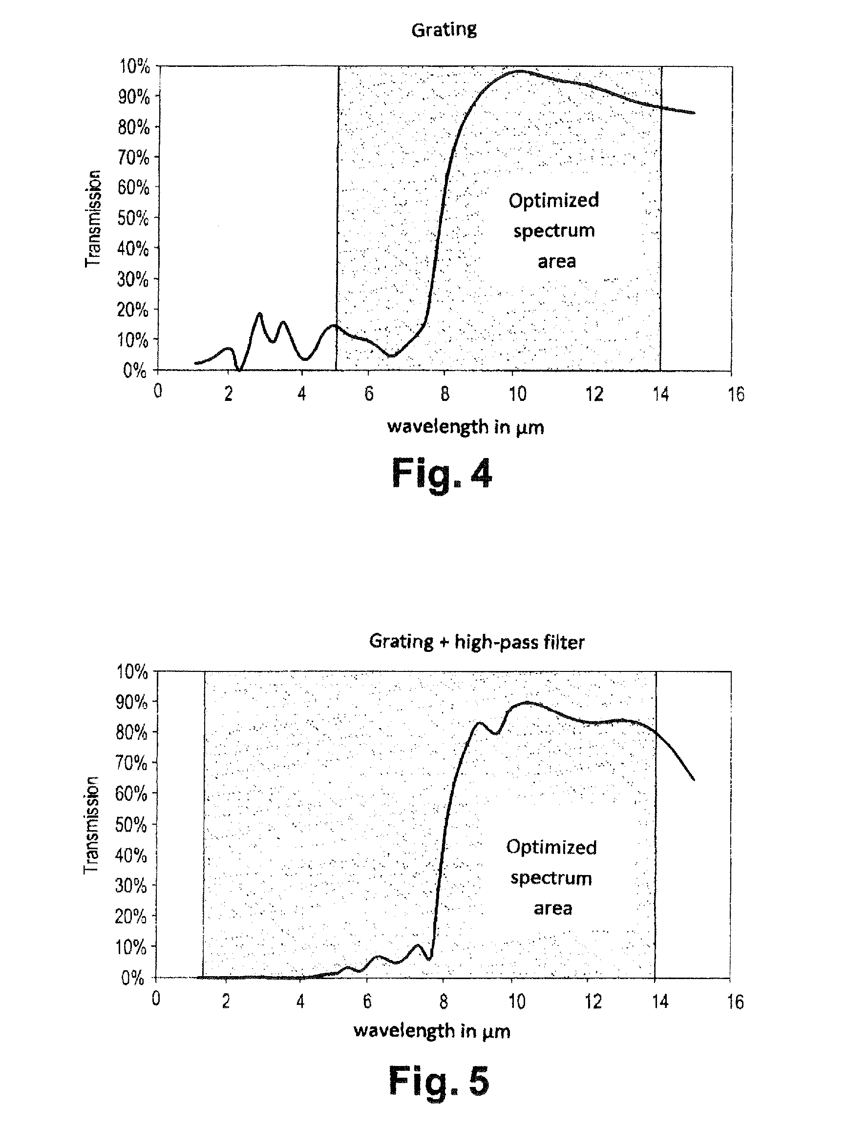
The present invention aims to provide an infrared bolometric detector with a window that has a filtering spectrum adapted for infrared bolometric detection, and is of very low defectivity. The invention solves the problem by using a diffraction filter instead of a multilayer interference filter, which results in a much easier industrial control of the quality of the assembly, and enables the manufacturing of components of decreased size, despite very harsh specifications as to the quality of the window. The use of mineral substrates transparent to infrared radiations, such as silicon or germanium, enables the use of micro-electronics-based technologies for the manufacturing of the diffraction filters, resulting in repeatability and quality higher than what is typically achieved by evaporation techniques. Diffraction filters can be formed using techniques of micro-electronic photolithography and raised or recessed patterns of the grating can be made very accurately using these techniques. The use of a diffraction filter provides better control over the low limit of the spectral bandwidth, resulting in greater flexibility in the construction of multilayer interference filters with lower thickness and number of layers, resulting in lower manufacturing cost and improved spectral transmission control with fewer defects.

Problems solved by technology

Indeed, such defects and imperfections are capable of disturbing the images formed by the detector, and this all the more as the filters are close to the focal plane, and thus to the sensitive detection elements.
However, such increasingly harsh specifications become an economical issue since the cost of these optical filters increases rapidly due to the specific method precautions to be taken and / or to the associated efficiency losses.
The obtained performance or the costs induced by this approach are not adapted yet to the need relative to the field of current infrared detection components.
Indeed, the number and the size of structure defects increase along with the filter thickness.
Thus, a decrease of their thickness results in a substantial decrease of the size and of the number of defects, as well as of the cost of the multilayer optical processing.
However, the decrease of the total thickness typically goes along with a decrease of the number of layers used, which necessarily results in a slackening of spectral transmission specifications.
This technique is however very seldom implemented, in particular due to the cost of the associated necessary techniques and instruments.
Further, the simplicity of such structures does not enable to define transmission spectrums such as desired for infrared bolometric detection.
Indeed, the equivalent of one or, at best, two interference layers is obtained in this manner, and only an antireflection function is thus obtained, which drastically limits the general optimization potential of the obtained filter.

Method used


Image

  • Infrared detector comprising a package integrating at least one diffraction grating
  • Infrared detector comprising a package integrating at least one diffraction grating
  • Infrared detector comprising a package integrating at least one diffraction grating

Examples


Embodiment Construction

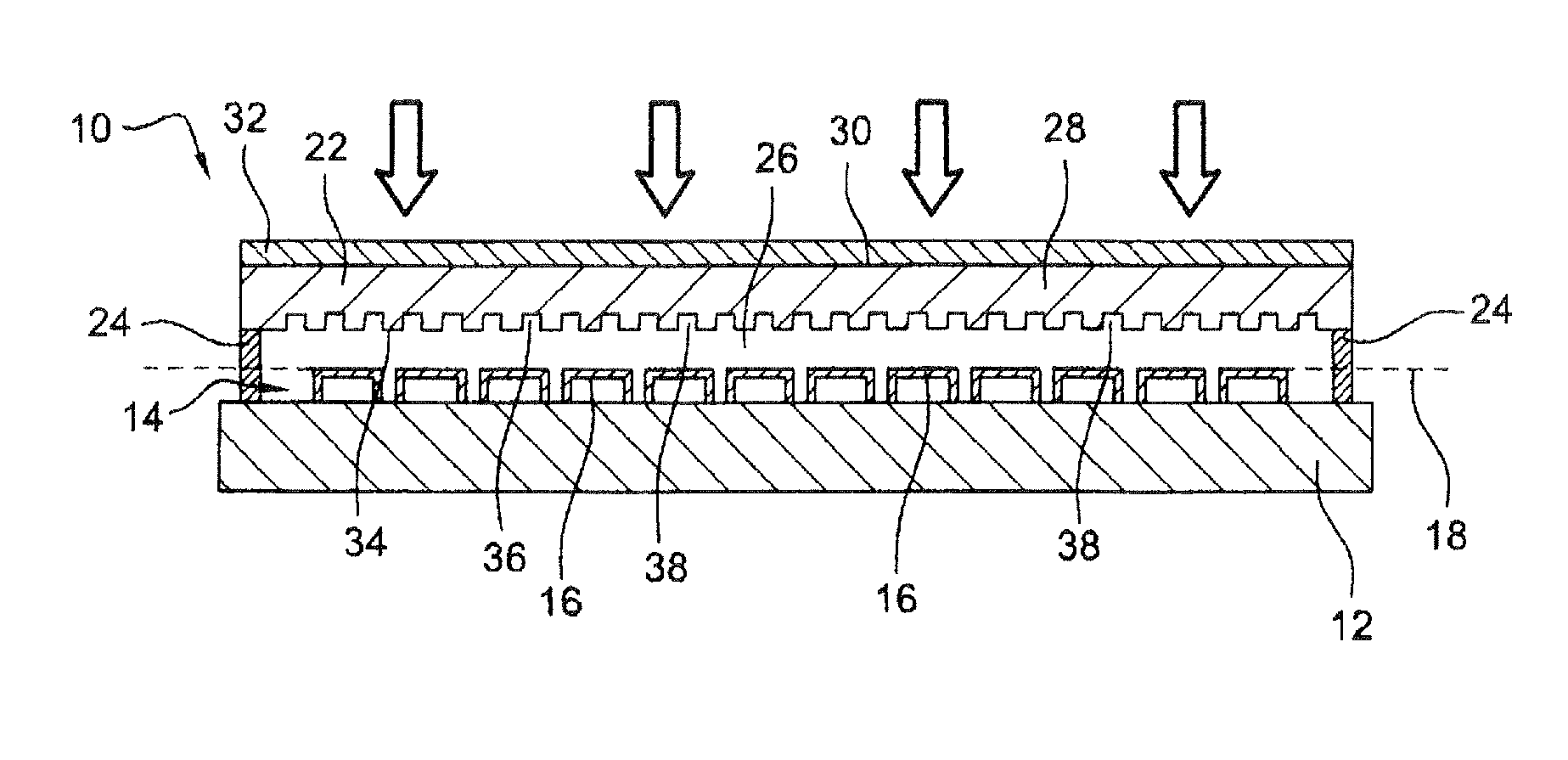
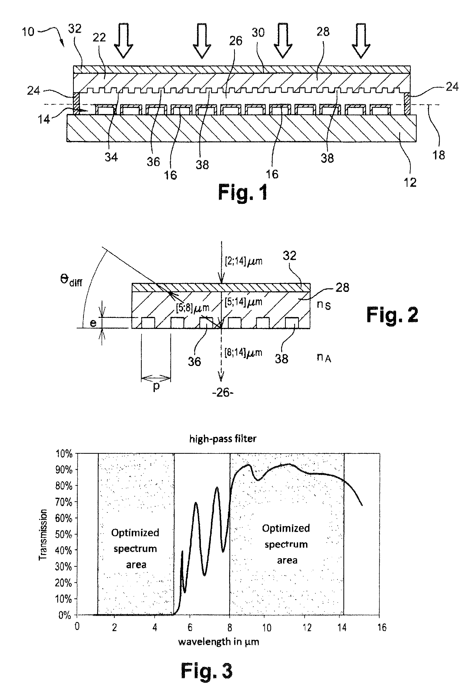
[0053]In FIG. 1, an infrared bolometric detector 10 comprises a base 12 comprising at its upper surface a read circuit, a sensitive retina 14, formed of a plurality of bolometric membranes 16 suspended above the read circuit by means of mechanical support, and thermal insulation arms. Membranes 16 each form a point of the detector sensitive to infrared radiation, especially of wavelength ranging between 8 μm and 14 μm. Retina 14 is placed in focal plane 18 of an optical system (not shown). The read circuit is not differentiated from base 12 in FIG. 1, where it forms this base per se, but may also be placed in the form of an electronic chip assembled on the internal surface of a bottom of a conventional package, the assembly forming base 12 according to the present invention. The read circuit further comprises addressing and bias circuits (also not shown) necessary to the forming of the useful signals by means of membranes 16.

[0054]Detector 10 further comprises a first wall 22, locat...


PUM


Abstract

The infrared detector includes a sensitive retina capable of detecting a radiation in the wavelength range between 8 and 14 micrometers; and a package containing the sensitive retina and including a window located opposite to the retina, said window comprising a substrate at least partially transparent in the wavelength range between 2 and 14 micrometers; and a set of optical filters formed on the window to attenuate an incident radiation on the retina in a wavelength range between 2 and 8 micrometers, and respectively an optical filter formed on a first surface of the window and attenuating the incident radiation in a first interval of the wavelength range between 2 and 8 micrometers, and a periodic diffraction grating formed on a second surface of the window and attenuating the incident radiation in a second interval of the wavelength range between 2 and 8 micrometers, different from the first interval.

Description

BACKGROUND OF THE INVENTION[0001]1. Field of the Invention[0002]The present disclosure relates to infrared detection or imaging, and especially to micro-bolometric detection. More specifically, the present invention relates to techniques enabling to adjust the spectral characteristics of packages containing the sensitive detection elements.[0003]2. Description of Related Art[0004]Detectors well known in the art intended for infrared imaging or thermography comprise a sensitive retina, placed in the focal plane of optics and integrated in a usually tight package, which protects the retina, and maintains it in a very low pressure envi-ronment usually necessary for it to operate properly. The retina is formed of a two-dimensional assembly of sensitive unit elements or “pixels”, formed at the surface of an electronic chip called “read circuit” (ROIC) comprising circuitry for addressing and forming the signal of each pixel. These signals altogether thus form the electric image in relatio...

Claims


Application Information

Patent Timeline
Patent Type & Authority Patents(United States)
IPC IPC(8): G01J3/02G01J5/08G02B5/18G02B5/20H01L27/146
CPCG01J5/0812H01L27/14625H01L27/14649H01L27/14618G01J5/0875G01J5/0862G02B5/203G02B5/1814G01J5/0803G02B5/208H01L2924/0002G01J5/0802H01L2924/00H01L27/14H01L31/09G01J5/0816
Inventor FAVIER, JEROME
Owner ULIS SAS
Learn More