
Spatial orientation of the carbon nanotubes in electrophoretic deposition process

a carbon nanotube and electrophoretic deposition technology, applied in the direction of basic electric elements, electrical apparatus, semiconductor devices, etc., can solve the problems of chaotic and disoriented bundles of nanotubes on the metal surface, and achieve the effect of simple, economic and versatil

Inactive Publication Date: 2014-07-22
NANO ELECTRONICS & PHOTONIC DEVICES & CIRCUITS
View PDF6 Cites 14 Cited by
  • Summary
  • Abstract
  • Description
  • Claims
  • Application Information

AI Technical Summary

Benefits of technology

The patent text discusses a method for placing nanotubes on metal surfaces using electrophoretic deposition, which is cost-effective and versatile. However, the main drawback is that this method typically results in the placement of chaotic and disoriented bundles of nanotubes on the metal surface. The patent aims to find a solution to produce arrays of individual nanotubes with controllable orientation and separation from each other, which would be highly desirable for future nanotube applications.

Problems solved by technology

The only significant deficiency of this technology is related to the fact that nanotube deposition results typically in a placement of chaotic and disoriented bundles of the nanotubes on the metal surface, see e.g. A. R. Boccaccini et al.

Method used


Image

  • Spatial orientation of the carbon nanotubes in electrophoretic deposition process
  • Spatial orientation of the carbon nanotubes in electrophoretic deposition process
  • Spatial orientation of the carbon nanotubes in electrophoretic deposition process

Examples


Embodiment Construction

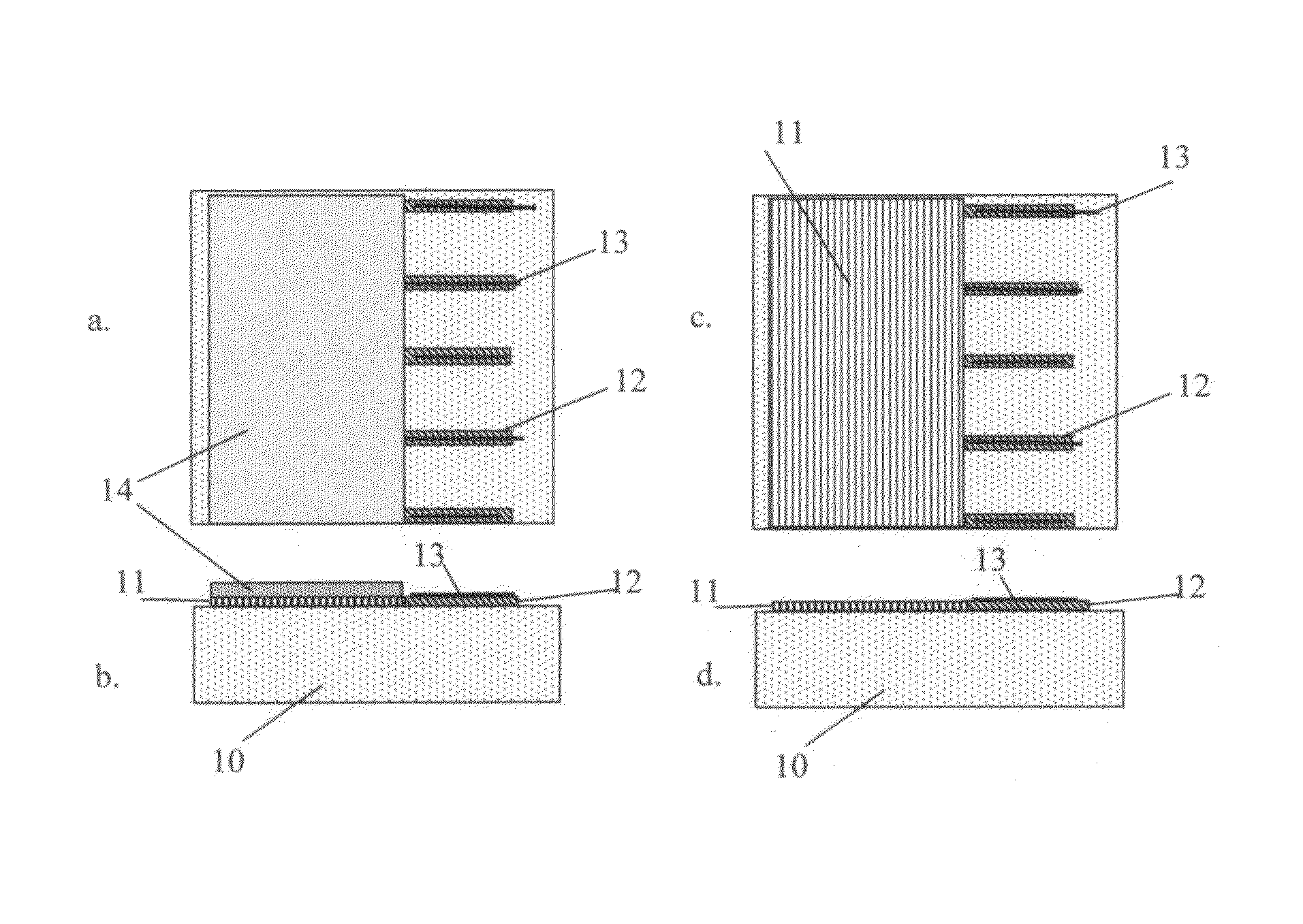
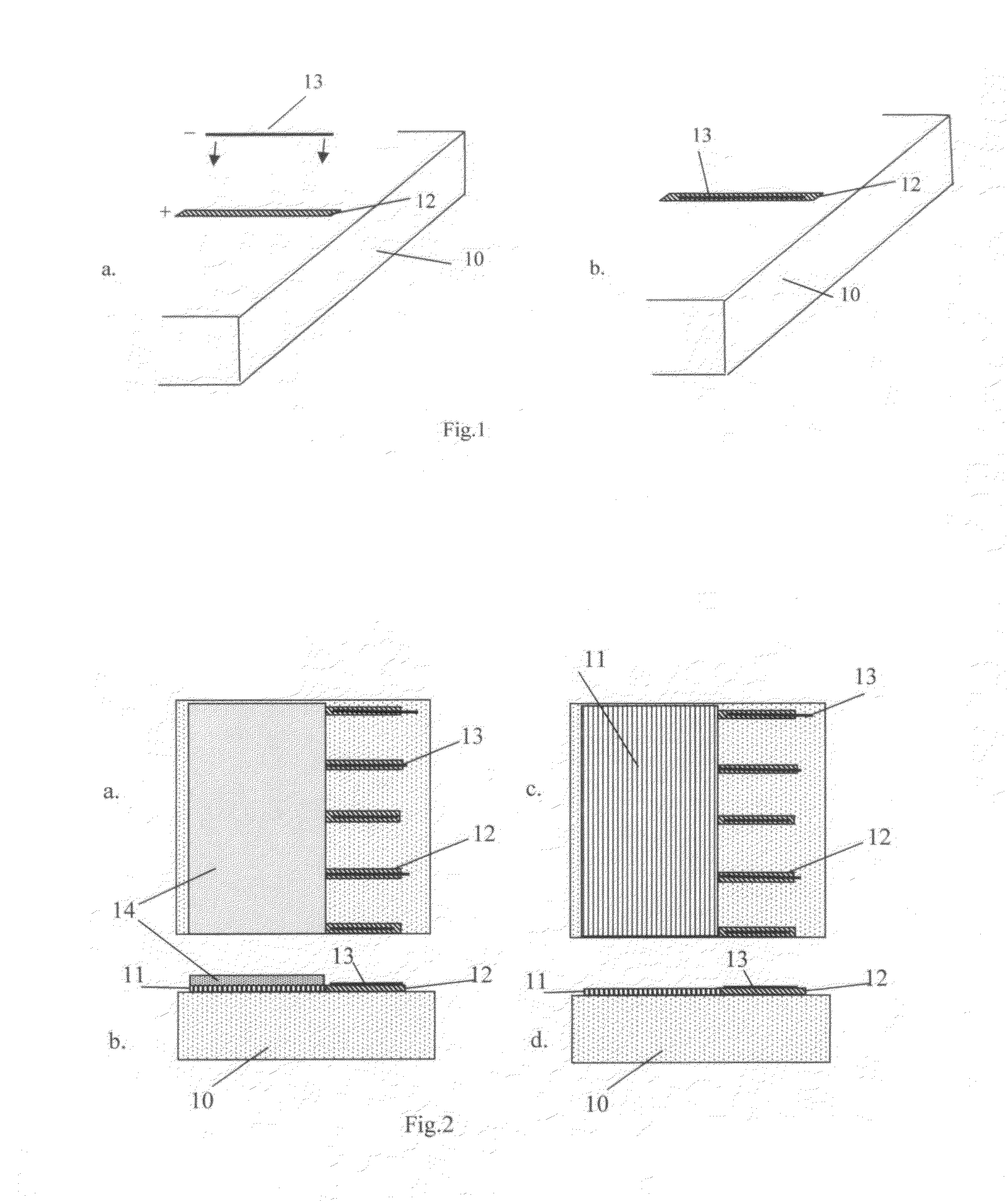
[0026]As discussed above, the main drawback of the original method of the electrophoretic deposition of the nanotubes results from a random orientation and positioning of the nanotubes on the metal electrode. A new electrophoretic method of the nanotube deposition, according to the present invention, offers placement of the nanotubes on the metal electrodes with the nanotube orientation parallel to the electrode length. This method eliminates all the above mentioned problems and make the EPD processing technique a reliable and simple method for CNT device technology.

[0027]FIG. 1 illustrates this method. The nanotube 13, carrying the electrostatic charge opposite to that of the elongated electrode 12 and having the length comparable to the electrode length, approaches the metal electrode 12 due to electrostatic metal-to-nanotube attraction. In this case, maximum electrode-to-nanotube capacitance occurs when nanotube is oriented parallel to the electrode length. This implies that the ...


PUM

PropertyMeasurementUnit
widthaaaaaaaaaa
widthaaaaaaaaaa
diameteraaaaaaaaaa

Abstract

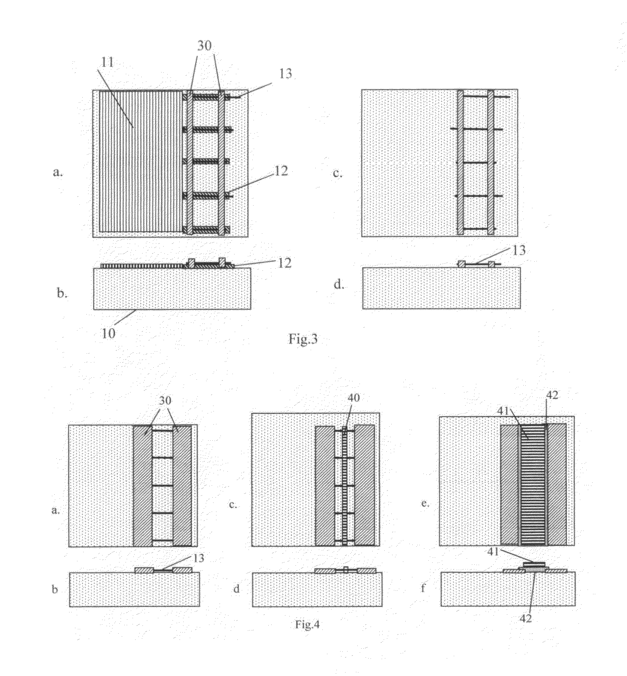
A new method of electrophoretic nanotube deposition is proposed wherein individual nanotubes are placed on metal electrodes which have their length significantly exceeding their width, while the nanotube length is chosen to be close to that of the metal electrode. Due to electrostatic attraction of individual nanotube to the elongated electrode, every nanotube approaching the electrode is deposited along the electrode, since such an orientation is energetically favorable. This method offers opportunity to produce oriented arrays of individual nanotubes, which opens up a new technique for fabrication and mass production of nanotube-based devices and circuits. Several such devices are considered. These are MESFET- and MOSFET-like transistors and CMOS-like voltage inverter.

Description

TECHNICAL FIELD[0001]The invention relates to formation of the arrays of individual nanotubes in the electrophoretic process of the nanotube deposition on the array of metal electrodes having a specifically selected geometry which causes a spatial orientation of the nanotubes placed on the electrodes. The oriented nanotube arrays are used to produce new technology for fabrication of electronic and photonic devices.BACKGROUND OF THE INVENTION[0002]The basic technological concept of the present invention is related to a spatial orientation of the individual nanotubes during the process of their electrophoretic deposition on the appropriately chosen metal electrodes. This simple and economical method of control of the nanotube placement can be used for making a mass production technology for nanotube-based electronic and photonic devices.[0003]Carbon nanotubes (CNT) possess unique properties that make them great candidates for future novel high-speed, high efficiency electronic and pho...

Claims


Application Information

Patent Timeline
Patent Type & Authority Patents(United States)
IPC IPC(8): H01L29/02
CPCH01L29/45H01L29/401H01L29/49H01L29/0673
Inventor KASTALSKY, ALEXANDER
Owner NANO ELECTRONICS & PHOTONIC DEVICES & CIRCUITS
Learn More