Method and apparatus for electron pattern imaging

a technology of electron pattern and electron pattern, applied in the field of electron pattern imaging, can solve the problems of diffraction characteristics of samples, insufficient beam current of most sems, and various deficiencies in current arrangement, and achieve the effect of safe operation of image intensifiers

Inactive Publication Date: 2014-05-27
EDAX
View PDF25 Cites 0 Cited by
  • Summary
  • Abstract
  • Description
  • Claims
  • Application Information

AI Technical Summary

Benefits of technology

[0013]An object of the present invention is to amplify light in an EBSD pattern collection system using an image intensifier in conjunction with a device for safely operating the image intensifier in an electron microscope environment.
[0016]Also provided is a method of electron pattern imaging. The method includes: positioning a device for converting electron patterns into visible light adjacent to a sample; positioning a first optical system downstream from the device for converting electron patterns into visible light; positioning a camera downstream from the first optical system; positioning an image intensifier between the device for converting electron patterns into visible light and the camera; positioning a device within the system for protecting the image intensifier from harmful light; receiving an electron backscatter diffraction (EBSD) pattern from a sample with the device for converting electron patterns into visible light such that the device for converting electron patterns into visible light converts the EBSD pattern to a corresponding light pattern; focusing the light pattern produced by the device for converting electron patterns into visible light with the first optical system; amplifying the light pattern produced by the device for converting electron patterns into visible light with the image intensifier; and obtaining an image of the light pattern with the camera. The device for protecting the image intensifier from harmful light is selected from the group consisting of: a near infrared (NIR) cut-off filter positioned upstream from the image intensifier for preventing NIR light from reaching the image intensifier, a light sensitive sensor in communication with a controller for detecting when a predetermined level of harmful light has been reached, and a short wavelength photo-cathode material positioned within the system to prevent excitation by NIR light.

Problems solved by technology

However, this current arrangement suffers from various deficiencies as discussed hereinafter.
Under low voltage and low current conditions, most SEMs do not provide sufficient beam current for optimal illumination of the phosphor screen.
Diffraction characteristics of the sample also create limitations in the current arrangement.
These conditions diffuse and / or weaken the diffraction pattern incident on the phosphor screen.
Geometric constraints limit the maximum size of lenses that can be used.
Within the given constraints of sample characteristics and current technology (SEM current, phosphor, and lens efficiency) exposure time to achieve an acceptable EBSD pattern is fundamentally limited by sensitivity and S:N of the camera.

Method used


Image

  • Method and apparatus for electron pattern imaging
  • Method and apparatus for electron pattern imaging
  • Method and apparatus for electron pattern imaging

Examples


Embodiment Construction

[0025]For purposes of the description hereinafter, the terms “upper”, “lower”, “right”, “left”, “vertical”, “horizontal”, “top”, “bottom”, “lateral”, “longitudinal”, and derivatives thereof shall relate to the invention as it is oriented in the drawing figures. However, it is to be understood that the invention may assume various alternative variations, except where expressly specified to the contrary. It is also to be understood that the specific devices illustrated in the attached drawings, and described in the following specification, are simply exemplary embodiments of the invention. Hence, specific dimensions and other physical characteristics related to the embodiments disclosed herein are not to be considered as limiting.

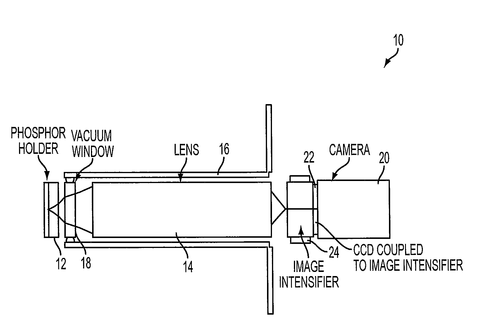
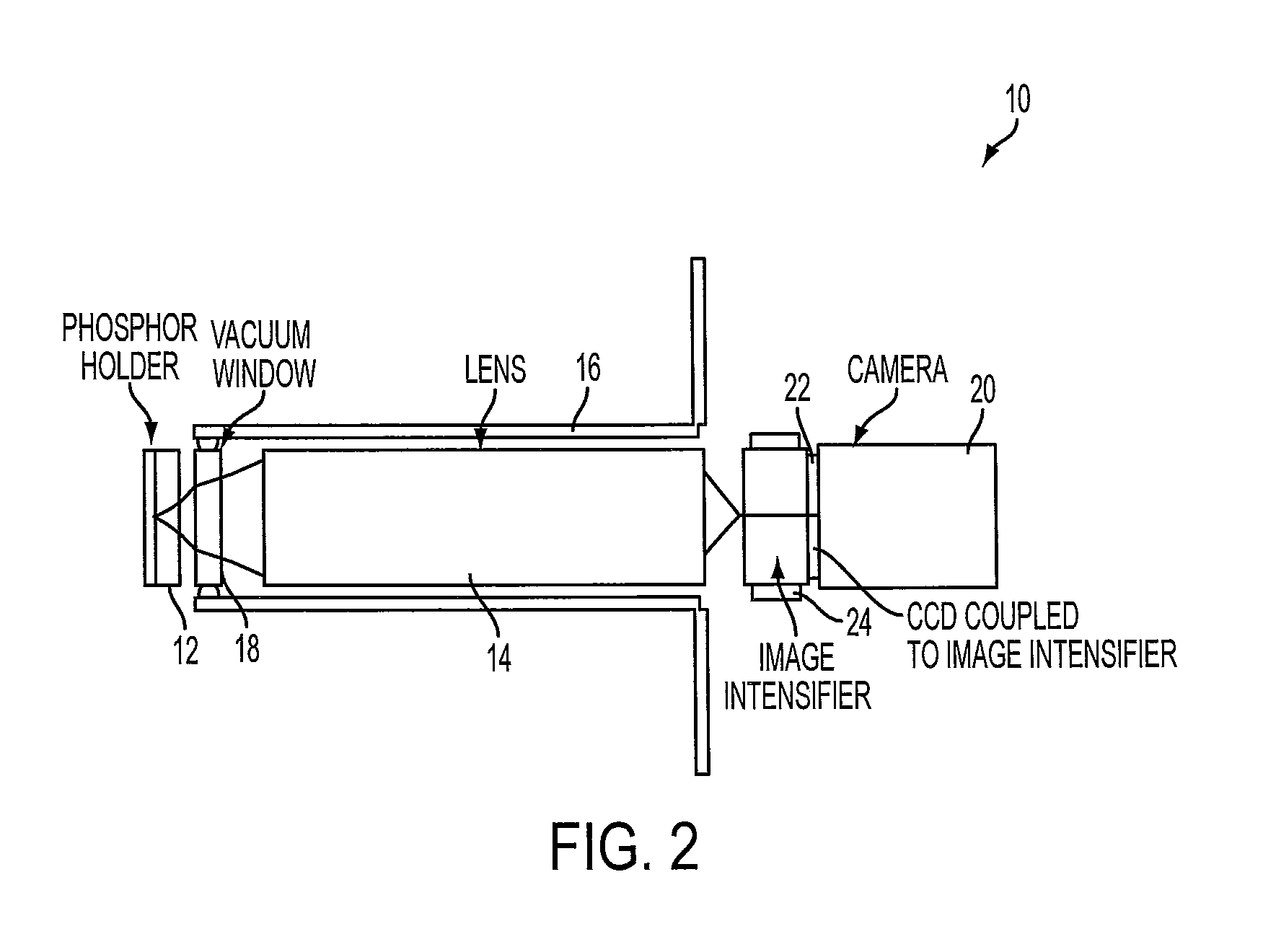
[0026]With reference to FIG. 2, a system for electron pattern imaging, denoted generally as reference numeral 10, includes: a device for converting electron patterns into visible light, such as a phosphor screen 12, provided to receive an electron backscatter...


PUM

PropertyMeasurementUnit
electron pattern imagingaaaaaaaaaa
wavelengthaaaaaaaaaa
scanning electron microscopeaaaaaaaaaa

Abstract

A system for electron pattern imaging includes: a device for converting electron patterns into visible light provided to receive an electron backscatter diffraction (EBSD) pattern from a sample and convert the EBSD pattern to a corresponding light pattern; a first optical system positioned downstream from the device for converting electron patterns into visible light for focusing the light pattern produced by the device for converting electron patterns into visible light; a camera positioned downstream from the first optical system for obtaining an image of the light pattern; an image intensifier positioned between the device for converting electron patterns into visible light and the camera for amplifying the light pattern produced by the device for converting electron patterns into visible light; and a device positioned within the system for protecting the image intensifier from harmful light.

Description

CROSS REFERENCE TO RELATED APPLICATIONS[0001]This application claims the benefit of U.S. Provisional Patent Application No. 61 / 663,102 entitled “Method and Apparatus for Electron Pattern Imaging” filed Jun. 22, 2012, which is hereby incorporated by reference in its entirety.BACKGROUND OF THE INVENTION[0002]1. Field of the Invention[0003]The present invention is generally directed to a method and apparatus for electron pattern imaging and, more specifically, to the use of an image intensifier to amplify light in an electron backscatter diffraction (EBSD) pattern collection system in a scanning electron microscope (SEM) environment.[0004]2. Description of Related Art[0005]In the field of material microanalysis, EBSD is used to study the microcrystalline characteristics of materials. The method uses the electron beam of an SEM incident on a sample and an electron imaging system to collect the electron diffraction pattern.[0006]With reference to FIG. 1, an example of a current arrangeme...

Claims


Application Information

Patent Timeline
Patent Type & Authority Patents(United States)
IPC IPC(8): G21K7/00G01N23/00
CPCH01J2237/2445H01J37/244H01J2237/24475H01J2237/2446
Inventor BUCHHOLD, REINHARDHAMMELL, BRENTNICOLOSI, JOSEPH A.DE KLOE, PETER ANTONIE
Owner EDAX
Why Eureka
Try Eureka