
Copper bonding wire for semiconductor device and bonding structure thereof

a technology semiconductor, which is applied in the direction of manufacturing tools, welding/cutting media/materials, and manufacturing tools, etc., can solve the problems of copper bonding wire, corrosion or the like, affecting the bonding strength, etc., and achieves superior long-term reliability and low material cost.

Active Publication Date: 2014-02-18
NIPPON STEEL CHEMICAL CO LTD +1
View PDF17 Cites 47 Cited by
  • Summary
  • Abstract
  • Description
  • Claims
  • Application Information

AI Technical Summary

Benefits of technology

The present invention provides a copper bonding wire for semiconductor that is cost-effective and has good reliability over the long-term, when used with Al electrodes. Additionally, this wire can be used in vehicle-mounted LSIs.

Problems solved by technology

However, since gold is expensive, there has been desired a bonding wire made of an other kind of metal that is inexpensive in terms of material cost.
However, a copper bonding wire imposes problems including: a decrease in a bonding strength due to an oxidation on a wire surface; and a tendency of causing corrosion or the like to occur on the wire surface when encapsulated by resin.
Those are also the reasons why the copper bonding wire has not yet been fully put to practical use in LSIs.
Since there are no past records indicating that the copper bonding wire has ever been used in LSIs, no full study has ever been carried out on, for example, a reliability of the copper bonding wire being used, thus leaving a standard for a reliability evaluation, a life or the like unclear.

Method used


Image

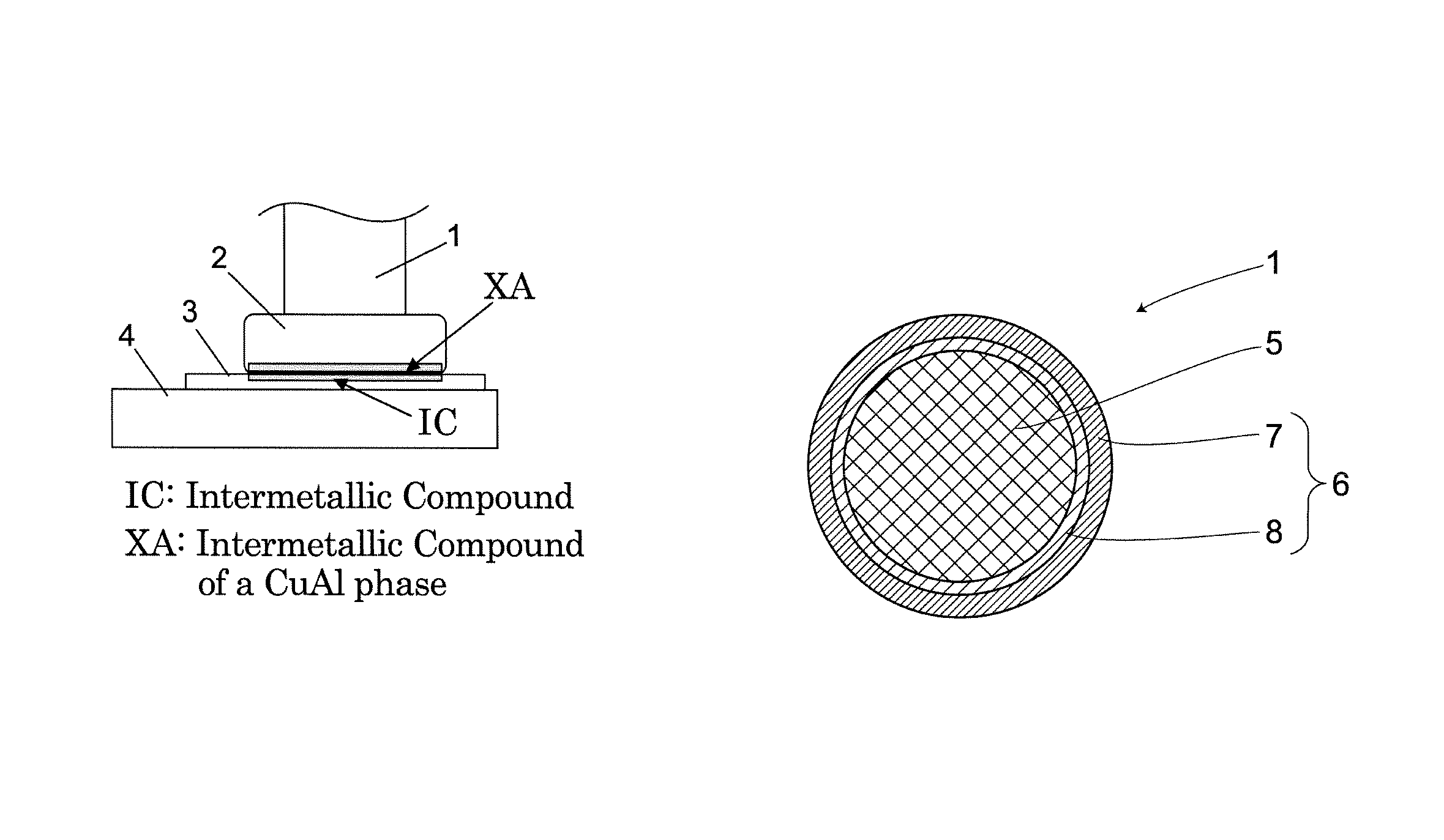
  • Copper bonding wire for semiconductor device and bonding structure thereof
  • Copper bonding wire for semiconductor device and bonding structure thereof
  • Copper bonding wire for semiconductor device and bonding structure thereof

Examples


working examples

[0099]Working examples are described hereunder.

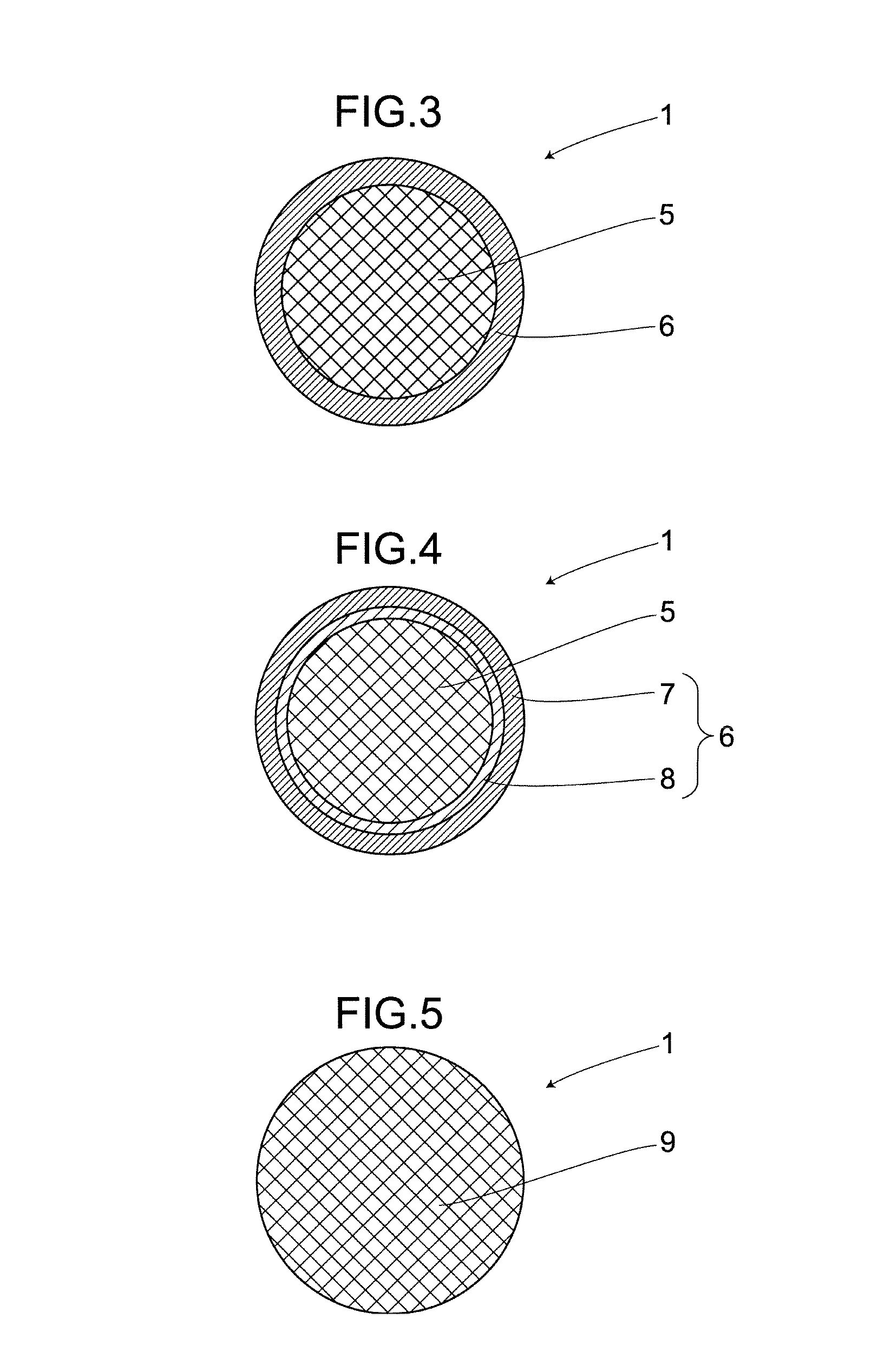
[0100]Raw materials of a copper bonding wire were as follows. As a core material, there was used Cu with a purity of not less than about 99.99% by mass, such Cu being an ultrapure material. Further, as an outer layer material, there was used Pd, Au or Ag with a purity of not less than 99.95% by mass, such Pd, Au or Ag being a highly pure material.

[0101]As for a monolayer copper bonding wire, there was manufactured an ingot by melting the ultrapure Cu to which a given alloy element(s) had been added. Here, a melting temperature was set to be 1100-1300° C. Further, rates at which the temperature rose and fell were controlled. Furthermore, as for an atmosphere, there were repeatedly performed vacuumization, inert gas replacement and the like. In this way, there could be controlled concentrations, distributions and the like of gas components in Cu.

[0102]When manufacturing a multilayer copper bonding wire, a copper wire having a wire diamete...


PUM

PropertyMeasurementUnit
temperatureaaaaaaaaaa
diameteraaaaaaaaaa
temperatureaaaaaaaaaa

Abstract

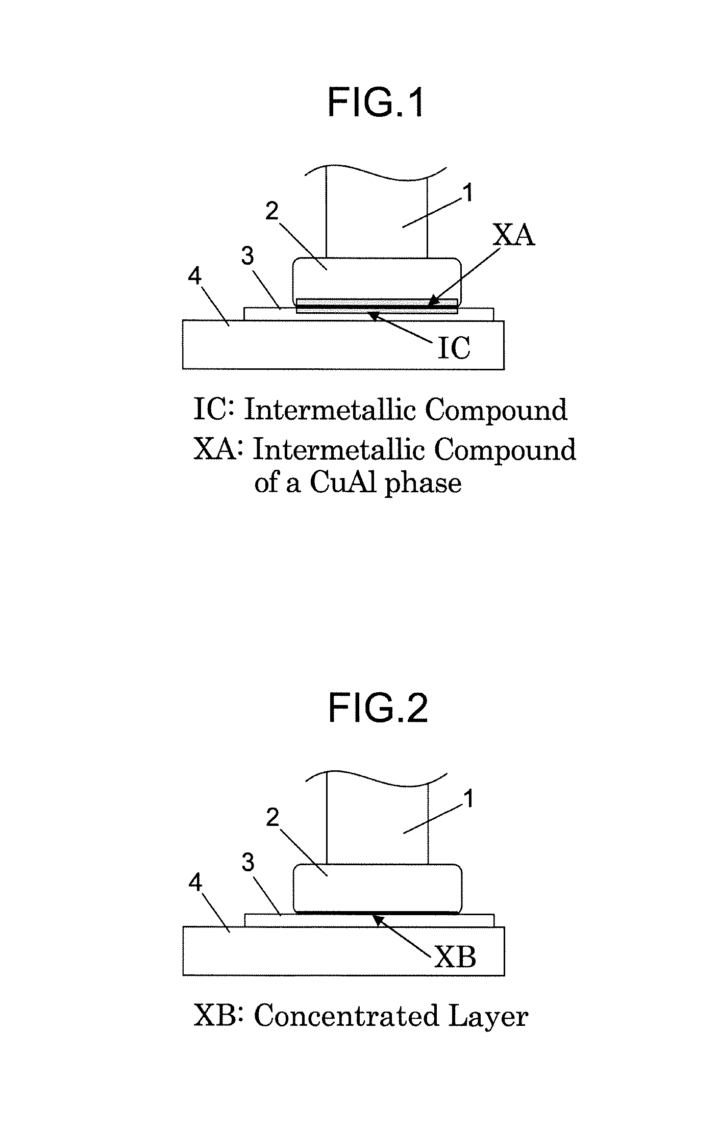
A bonding structure and a copper bonding wire for semiconductor device include a ball-bonded portion formed by bonding to the aluminum electrode a ball formed on a front end of the copper bonding wire. After being heated at any temperature between 130° C. and 200° C., the ball-bonded portion exhibits a relative compound ratio R1 of 40-100%, the relative compound ratio R1 being a ratio of a thickness of a Cu—Al intermetallic compound to thicknesses of intermetallic compounds that are composed of Cu and Al and formed on a cross-sectional surface of the ball-bonded portion.

Description

RELATED APPLICATIONS[0001]This application is the U.S. National Phase under 35 U.S.C. §371 of International Application No. PCT / JP2011 / 052270, filed on Feb. 3, 2011, which in turn claims the benefit of Japanese Application No. 2010-021971, filed on Feb. 3, 2010, the disclosures of which Applications are incorporated by reference herein.TECHNICAL FIELD[0002]The present invention relates to a copper bonding wire for semiconductor and a bonding structure thereof.BACKGROUND ART[0003]Nowadays, as a bonding wire (a wire used for connection in a wire bonding method) for connecting an electrode on a semiconductor device and an external terminal, there is mainly used a thin wire (bonding wire) having a wire diameter of about 13-50 μm. Wire bonding is generally performed through a thermocompression bonding method with the aid of ultrasonic waves. Here, there are used, for example, a general bonding device and a capillary jig allowing a bonding wire to be passed thereinside when performing bon...

Claims


Application Information

Patent Timeline
Patent Type & Authority Patents(United States)
IPC IPC(8): H01L23/49
CPCH01L2924/01074H01L2924/01006H01L2224/48463H01L2224/48799H01L24/85B23K35/3046H01L2924/01004H01L2924/01327C22F1/08H01L2924/01082H01L2924/01046C22C9/00H01L2224/48453H01L2924/01015H01L24/45C23F17/00H01L2924/01005H01L2924/01033H01L2924/01047H01L2224/05624H01L2924/01019H01L2924/01079B23K35/0244H01L2224/48507H01L2924/01013H01L2924/10253H01L24/48H01L2924/01078H01L2224/45147H01L2924/01045H01L2224/45565H01L2924/01014H01L2924/20105H01L2224/85H01L2924/01029H01L2924/20104H01L24/05H01L2224/04042H01L2224/45015H01L24/43H01L2224/43848H01L2224/45639H01L2224/45644H01L2224/45664H01L2224/48824H01L2224/85203H01L2224/85205H01L2924/00011H01L2924/181H01L2924/01032H01L2924/00012H01L2924/00H01L2924/013H01L2924/20751H01L2924/20752H01L2924/20753H01L2924/20754H01L2924/20755H01L2924/20756H01L2924/20757H01L2924/01049H01L2924/01203H01L2924/00013H01L2924/01204H01L2924/00014
Inventor UNO, TOMOHIROYAMADA, TAKASHIIKEDA, ATSUO
Owner NIPPON STEEL CHEMICAL CO LTD
Learn More