
Method for producing nanostructures on metal oxide substrate, method for depositing thin film on same, and thin film device

Inactive Publication Date: 2013-06-11
ECOLE POLYTECHNIQUE +2
View PDF0 Cites 0 Cited by
  • Summary
  • Abstract
  • Description
  • Claims
  • Application Information

AI Technical Summary

Benefits of technology

The invention describes a process for growing nanostructures on a substrate without the need for a step of depositing and positioning metal catalyst aggregates on the substrate. Instead, metal aggregates are directly obtained from the metal oxide of the substrate. This process has advantages such as avoiding pollution and oxidation, shorter growth time, better control, and reduced equipment requirements. The use of plasmas and low-melting point metals also reduces the temperature during the treatment, making it compatible with a wider range of substrates and reducing costs. Additionally, the process allows for the rapid production of nanostructures on large surface areas.

Problems solved by technology

Most of such methods for producing nanostructures on a substrate require heavy equipments, and can not be applied to large surfaces.
They can neither be carried out in situ, except for the method of evaporating the metal layer, which, on the other hand, requires a complex installation.
Such transfer causes pollution or oxidation of the catalysts in contact with air, as well as loss of time (operations of loading / unloading, pumping, etc. . . . ).
There is no known method that permits to grow nanostructures of a chemical element such as silicon directly on a metal oxide substrate.

Method used


Image

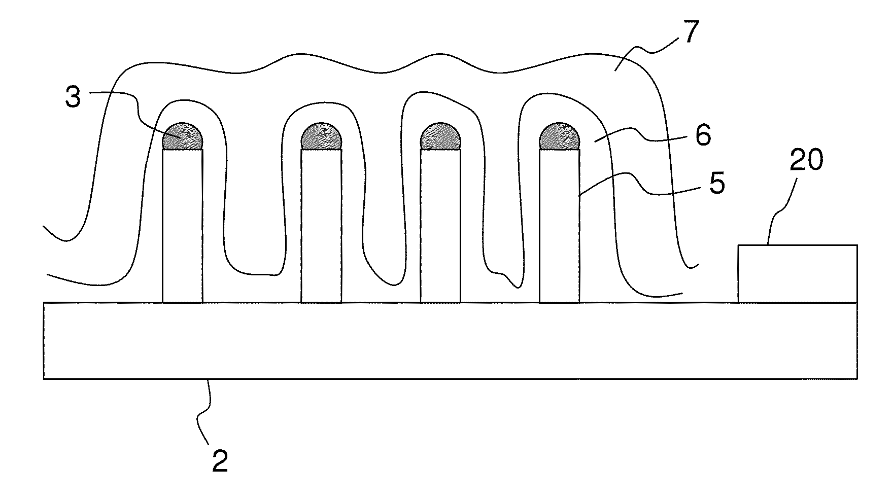
  • Method for producing nanostructures on metal oxide substrate, method for depositing thin film on same, and thin film device
  • Method for producing nanostructures on metal oxide substrate, method for depositing thin film on same, and thin film device
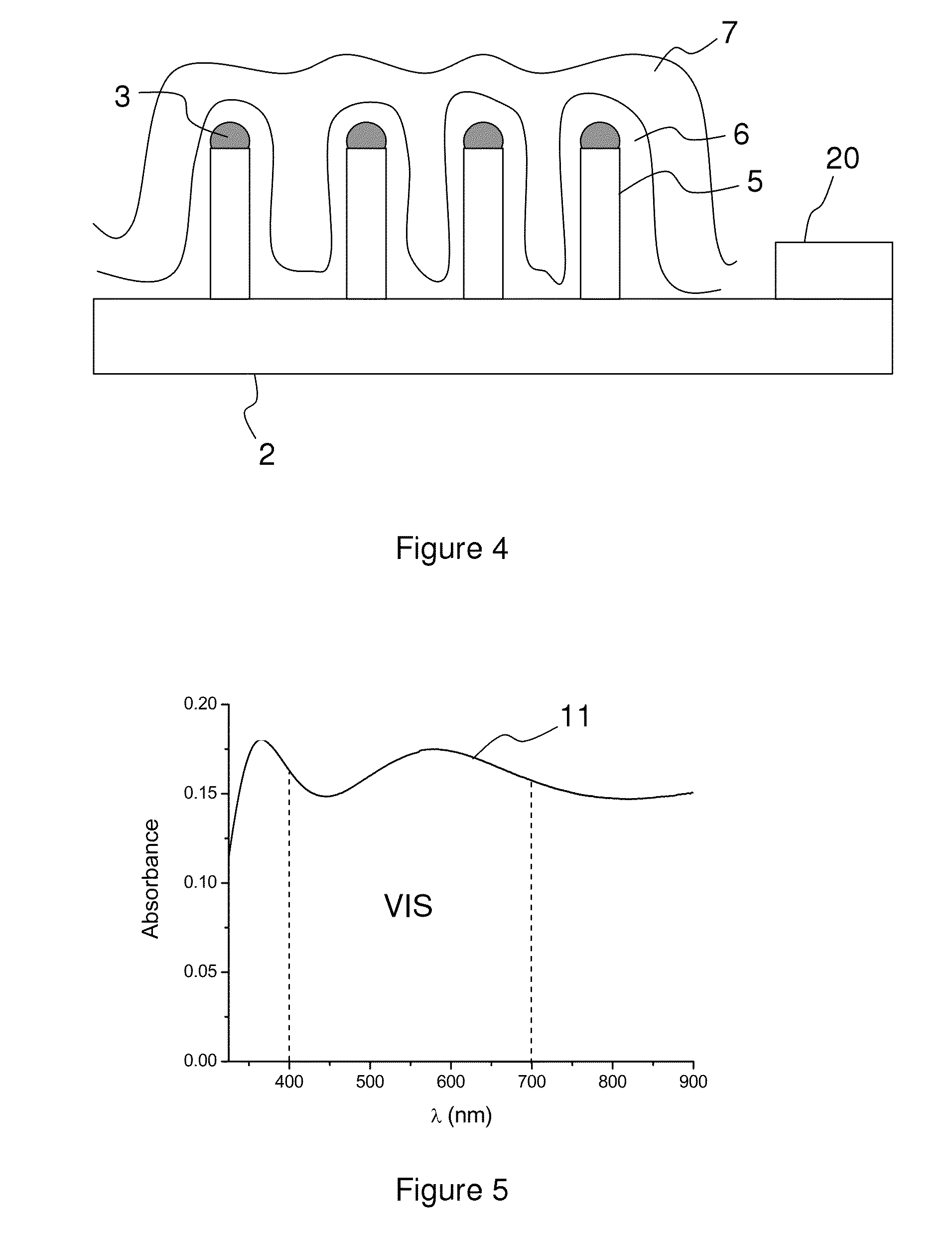
  • Method for producing nanostructures on metal oxide substrate, method for depositing thin film on same, and thin film device

Examples


Embodiment Construction

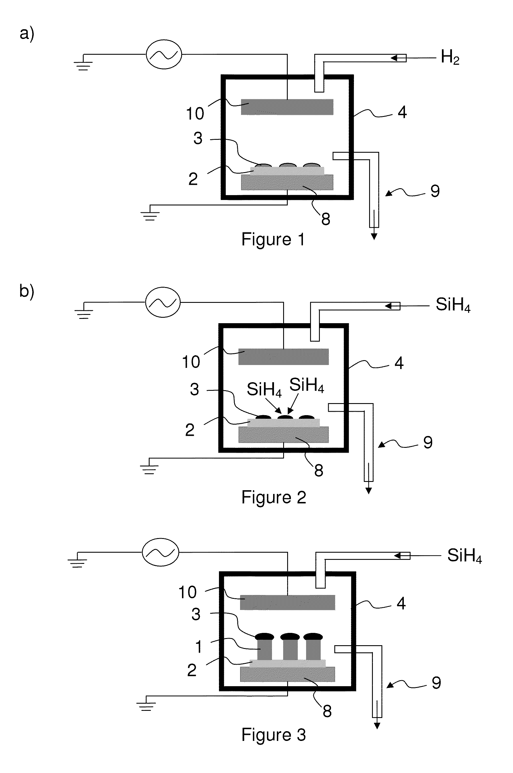
[0067]FIG. 1 illustrates a plasma reactor in which the first step of forming metal aggregates on a metal oxide substrate is carried out, according to an embodiment of the invention.

[0068]In this example, this plasma reactor is a radiofrequency plasma-enhanced chemical vapour deposition (PECVD-RF) reactor. It is also possible to use other types of plasma reactors (for example, VHF, microwave . . . ) and other operating conditions.

[0069]The metal oxide substrate 2 is composed of a glass or polymer substrate or other, covered with a thin-film metal oxide layer.

[0070]The deposition of the metal oxide layer may be obtained by different techniques of deposition, such as pyrolysis, sputtering, chemical vapour deposition (CVD), etc. . . . .

[0071]The metal oxide layer may be optically transparent or not, and have optical and conductive properties.

[0072]After a conventional cleaning of the metal oxide substrate 2 (solvent baths), the latter is introduced into the chamber of the plasma reactor...


PUM

PropertyMeasurementUnit
Temperatureaaaaaaaaaa
Timeaaaaaaaaaa
Pressureaaaaaaaaaa

Abstract

A method for producing nanostructures on a metal oxide substrate includes the following steps: a) forming metal aggregates on the metal oxide substrate; and b) vapor phase growing nanostructures on the metal oxide substrate covered with metal aggregates, the substrate being heated in the presence of one or more precursor gases, and the vapor phase growth of nanostructures being catalyzed by the metal aggregates. The metal aggregate formation stage a) includes an operation for reducing the surface of the metal oxide substrate by reductive plasma treatment, causing droplets of metal aggregates to form on the substrate, the metal aggregate formation stage a) and the nanostructure growth stage b) being carried out in series in a single shared plasma reactor chamber, the nanostructure growth being directly carried out on the droplets of metal aggregates.

Description

FIELD OF THE INVENTION[0001]The present invention relates to a process of producing nanostructures on a metal oxide substrate, a process of growing thin-film layers on such a substrate, and a thin-film device.BACKGROUND OF THE INVENTION[0002]The quasi-one-dimensional nanostructures, such as carbon nanotubes or semiconductor nanowires, are used in particular in the field of electronics (for example, thin-film transistors), in the field of optoelectronics (for example, solar cells, electroluminescent diodes), and as sensors because of their original properties (optical, electronic, thermal, mechanical) and their large specific surface area.[0003]These nanostructures are obtained by being grown or deposited on a substrate that, in the field of optoelectronics, is preferentially both transparent and conductor of electricity. Such a substrate may be obtained by applying a thin-film layer of metal oxide as, for example, tin oxide (SnO2) or tin-doped indium oxide (ITO, “indium tin oxide”),...

Claims


Application Information

Patent Timeline
IPC IPC(8): H01L21/20
CPCB82Y10/00B82Y30/00C30B25/18C30B29/04C30B29/06H01L31/0352C30B29/36C30B29/38C30B29/52C30B29/605C30B29/08B81B2203/0361B81C1/00031B82Y40/00C01B21/0682C01B33/027C01B33/029C23C16/0218C23C16/24C23C16/46C30B11/12C30B25/00C30B29/60C01B32/05H01L21/02532H01L21/02576H01L21/02579H01L21/02603H01L21/0262H01L21/02645H01L21/02653H01L29/0676H01L29/66439H01L29/775
Inventor ALET, PIERRE-JEANROCA I CABAROCCAS, PERE
Owner ECOLE POLYTECHNIQUE
Learn More