Semiconductor device test circuit, semiconductor device, and its manufacturing method

a semiconductor device and test circuit technology, applied in the field of test circuits, can solve the problems of insufficient inability to fix the potential level in each of the internal nodes, and insufficient toggling the output of such a f/f circuit that cannot be included in a scan chain, so as to suppress the overhead of the semiconductor circuit and the effect of the semiconductor circuit overhead

Inactive Publication Date: 2013-03-26
RENESAS ELECTRONICS CORP
View PDF12 Cites 0 Cited by
  • Summary
  • Abstract
  • Description
  • Claims
  • Application Information

AI Technical Summary

Benefits of technology

[0011]According to the present invention, therefore, it is possible to dispose this test circuit for a node to which a stress cannot be applied only with use of an F / F circuit, thereby the stress can be applied to the node. Furthermore, because this test circuit is disposed in the subject semiconductor device so as to be connected to a combinational circuit therein, the semiconductor circuit overhead can be suppressed.
[0012]This is why the present invention can provide a test circuit, a semiconductor device, and its manufacturing method, each of which enables a stress to be applied to each node of each object combinational circuit to which such a stress cannot be applied only with use of an F / F circuit and enables the semiconductor circuit overhead to be suppressed when in burn-in or leak test operation for the semiconductor device.

Problems solved by technology

However, a burn-in test, if a scan path test is included in that, can activate each circuit in the subject semiconductor device at a high percentage, but there are still some inactive circuits left over in the combinational circuit connected to an F / F circuit that is not included in the scan chain.
In this case, however, even when a huge number of scan patterns are generated for a large-scale semiconductor in recent years, it is still difficult to fix the potential level in each of the internal nodes of the subject combinational circuit disposed in a deep layer from the external terminal and the F / F circuit.
Similarly, simple toggling of the output of such an F / F circuit that cannot be included in a scan chain is insufficient for the consideration to the logic of the combinational circuit that receives the output from the F / F.
This is why the conventional techniques cause some inactive combinational circuits to be left over.
And if a node is provided with many test F / F circuits, the semiconductor circuit overhead increases significantly.
And it is difficult to add test F / F circuits to such an inactive node one by one.

Method used


Image

  • Semiconductor device test circuit, semiconductor device, and its manufacturing method
  • Semiconductor device test circuit, semiconductor device, and its manufacturing method
  • Semiconductor device test circuit, semiconductor device, and its manufacturing method

Examples


first embodiment

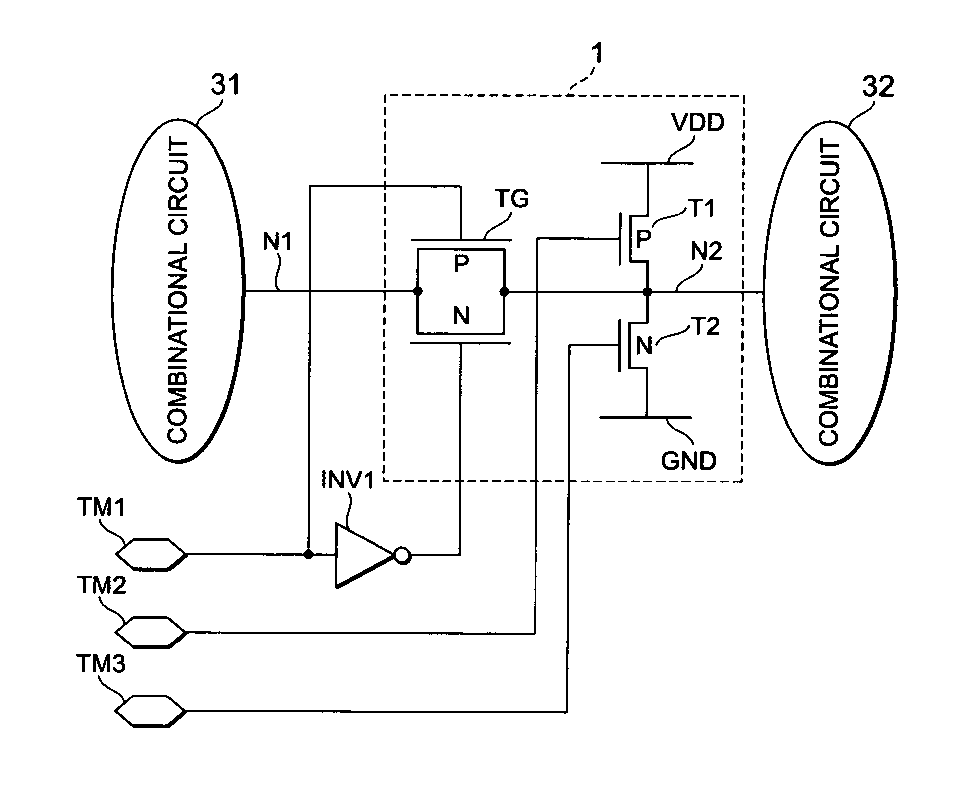
[0037]At first, there will be described a configuration of a test circuit 1, as well as configurations of its peripheral circuits in the first embodiment of the present invention with reference to the block diagram shown in FIG. 1. The test circuit 1 includes a transfer gate switch TG consisting of a PMOS (Positive-channel Metal Oxide Semiconductor) transistor and an NMOS (Negative-channel Metal Oxide Semiconductor) transistor. The test circuit 1 also includes a first transistor (PMOS) T1 connected between a power supply VDD and a node N2 and a second transistor (NMOS) T2 connected between a ground GND and the node N2.

[0038]The node N1 connected to a combinational circuit 31 and the node 2 connected to another combinational circuit 32 are connected to each other through the transfer gate switch TG. A test mode control terminal TM1 is connected to the PMOS transistor of the transfer gate switch TG so as to have a positive logic and to the NMOS transistor so as to have an inverted log...

second embodiment

[0050]Next, there will be described a configuration of a test circuit 1 and configurations of its peripheral circuits in this second embodiment with reference to the block diagram shown in FIG. 3. The test circuit 1 is the same in configuration as that shown in FIG. 1, so that its description will be omitted here.

[0051]A node N1 connected to a combinational circuit 31 and another node N2 connected to another combinational circuit 32 are connected to each other through a transfer gate switch TG. A test mode control terminal TM1 is connected to a PMOS transistor of the transfer gate switch TG and a test decoder TD so as to have a positive logic respectively while the test mode control terminal TM1 is connected to an NMOS transistor of the transfer gate switch TG so as to have an inverted logic generated by an inverter logic block INV1. The test mode control terminal TM2 is connected to the test decoder TD. The test decoder TD is connected to the first transistor T1 through a test deco...

third embodiment

[0066]In this third embodiment of the present invention, the test mode control terminal TM2 used in the second embodiment is replaced with a scan clock terminal CLK.

[0067]At first, there will be described a configuration of a test circuit 1 and configuration of its peripheral circuits with reference to the block diagram shown in FIG. 7. In FIG. 7, the test mode control terminal TM2 shown in FIG. 3 is replaced with a scan clock terminal CLK as described above. Other components are the same as those shown in FIG. 3, so that the description for them will be omitted here.

[0068]Also in the test decoder TD shown in FIG. 8, the test mode control terminal TM2 shown in FIG. 4 is replaced with a scan clock terminal CLK. Other parts are the same as those shown in FIG. 4, so that the description for them will be omitted here.

[0069]Next, there will be described a configuration of a test circuit 1 that includes a built-in test circuit 1 with reference to the clock diagram shown in FIG. 10. In the...


PUM


Abstract

The test circuit can apply a stress to each node of each object combinational circuit in the semiconductor device and suppress the semiconductor circuit overhead when in burn-in or leak test operations for the semiconductor device while it has been impossible to apply such a stress to any of such nodes only with use of an F / F circuit in any conventional environments. The test circuit is disposed in the semiconductor and combined with first and second combinational circuits therein. In the semiconductor device, a transfer gate switch is connected between first and second nodes and a first transistor is connected between the second node and a power supply. The second transistor is connected between the second node and a ground. Each of the transfer gate switch and the first and second transistors operates according to at least one of the control signals supplied from outside the semiconductor device.

Description

FIELD OF THE INVENTION[0001]The present invention relates to a test circuit to be used for burn-in and leak tests and more particularly to a circuit that applies a stress to each node of each object combinational circuit when in such burn-in and leak tests.BACKGROUND OF THE INVENTION[0002]In recent years, the reliability requirements of semiconductor devices have been set higher and higher. And in order to meet such requirements, there have been invented and employed various test methods and test circuits. Among those test methods, there is a burn-in test, which applies a stress to each object semiconductor device so as to quicken the appearance of physical deterioration and detects semiconductors having latent trouble factors as defective ones. There is also a leak test employed often to detect a short circuit between a signal wiring and another signal wiring or power wiring as an increase of the supply current.[0003]In case of burn-in tests, it is considered to be ideal to apply a...

Claims


Application Information

Patent Timeline
Patent Type & Authority Patents(United States)
IPC IPC(8): G01R31/28
CPCG01R31/318577
Inventor ISHIZUKA, SATOSHI
Owner RENESAS ELECTRONICS CORP
Why Eureka
Try Eureka