Electronic device

a technology of electronic devices and connected parts, applied in the direction of coupling device connections, support structure mounting, electrical apparatus, etc., can solve the problems of damage to the connected portions and possibly the electronic devices in turn, and achieve the effect of reducing stress and reducing the stress applied to the connected portions between the casing and the circuit board

Inactive Publication Date: 2019-10-31
FANUC LTD
View PDF14 Cites 2 Cited by
  • Summary
  • Abstract
  • Description
  • Claims
  • Application Information

AI Technical Summary

Benefits of technology

[0006]Accordingly, an object of the present invention is to reduce stress applied to connected portions between a casing and a circuit board in an electronic device in which the circuit board is inserted in a slot of the casing.
[0007]According to an aspect of the present invention, an electronic device includes: a casing having a slot formed therein; a circuit board configured to be inserted in the slot; a first connector provided at an end of the circuit board in an insertion direction; a second connector provided in the casing and configured to be fitted with the first connector when the circuit board is inserted in the slot; pairs of guide rails provided in the slot in correspondence respectively with both ends of the circuit board in a direction intersecting the insertion direction, so as to guide insertion of the circuit board into the slot, each pair of the guide rails including a first guide rail and a second guide rail that are provided in the slot so as to extend along the insertion direction respectively on both surface sides of the circuit board inserted in the slot; and a pair of pressing members configured to, when the circuit board is inserted in the slot, press the circuit board so as to hold and sandwich the circuit board therebetween. According to the present invention, the circuit board is fixed in the casing by being pressed by the pair of pressing members, and as a result the stresses applied to the connected portions between the casing and the circuit board are reduced.

Problems solved by technology

As a result, the stresses applied to the connected portions act as loads, which may damage the connected portions and possibly the electronic device in turn.

Method used


Image

  • Electronic device
  • Electronic device
  • Electronic device

Examples


first embodiment

Configuration of First Embodiment

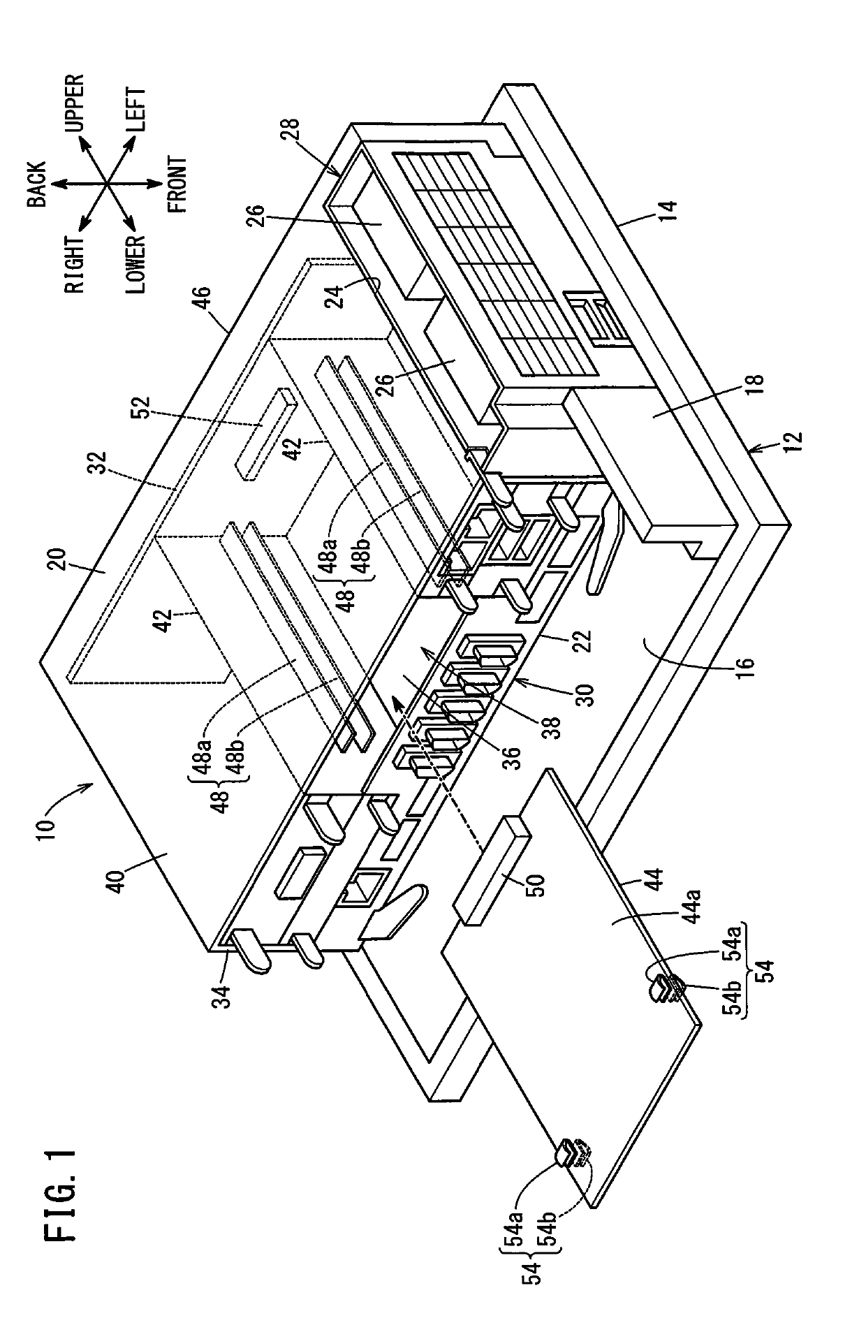
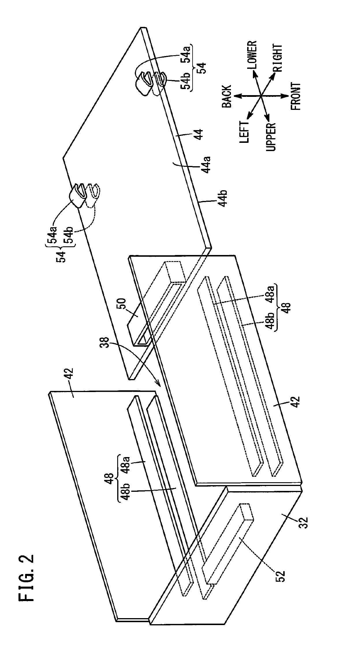
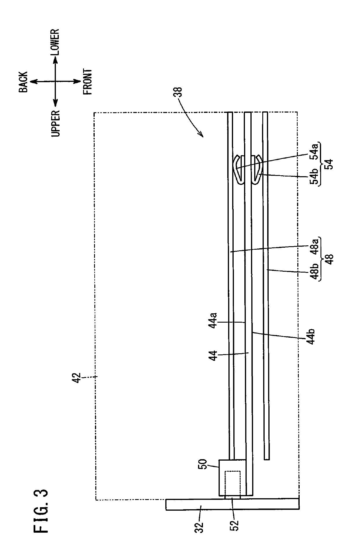
[0018]FIG. 1 is a perspective view showing the configuration of the entirety of an electronic device 10 according to a first embodiment.

[0019]As shown in FIG. 1, the electronic device 10 of this embodiment is a control device for controlling a machine tool, robot, injection molding machine, or wire electric discharge machine, for example. The electronic device 10 is provided to an indicator 12. The indicator 12 is a display unit, for example, and a liquid-crystal screen (not shown) is provided on a front surface 14 of the indicator 12. The screen of the indicator 12 need not necessarily be liquid crystal.

[0020]In the description below, the directions are indicated as up-down (upper-lower), right-left, and front-back directions seen from the front of the display screen of the indicator 12.

[0021]In the example of FIG. 1, the electronic device 10 and a user interface unit 18, which is connectable to external equipment (not shown), are detachably mounted...

second embodiment

Configuration of Second Embodiment

[0055]An electronic device 10 according to a second embodiment will now be described. The same constituent elements as those described in the first embodiment will be labeled by using the same reference numerals and overlapping descriptions will not be repeated.

[0056]FIG. 6 is a perspective view showing the configuration of part of the electronic device 10 of the second embodiment. FIG. 7 is a perspective view showing a state in which the circuit board 44 is being inserted in the slot 38 of the electronic device 10 of the second embodiment.

[0057]As shown in FIGS. 6 and 7, in the electronic device 10 of this embodiment, a pair of pressing members 56 are provided respectively between the wall surfaces (partition plates42) of the slot 38 and the circuit board 44. That is, in this embodiment, a first pressing member 56a is disposed between one end 44c of both ends of the circuit board 44 in the right-left direction and a wall surface of the slot 38 that...

first modification

(First Modification)

[0065]FIG. 8 is a perspective view showing the configuration of part of an electronic device 10 according to a first modification of the second embodiment.

[0066]For example, as shown in FIG. 8, a pair of pressing members 56 may be fixed respectively to one end 44c and the other end 44d of the circuit board 44. In this case, when the pair of pressing members 56 are bent in a U-shape as shown in FIG. 8, for example, the distal ends of the pair of pressing members 56 are directed in the direction opposite to the insertion direction of the circuit board 44 (directed in the direction to the lower side), and then, when the circuit board 44 is inserted into the slot 38, the pair of pressing members 56 are prevented from being caught on the edges of the opening 36 of the slot 38, and thus the insertion of the circuit board is not hindered.


PUM


Abstract

An electronic device includes: a casing having a slot; a circuit board; a first connector provided at an end of the circuit board in an insertion direction; a second connector provided in the slot and configured to be fitted with the first connector when the circuit board is inserted in the slot; pairs of guide rails provided in the slot in correspondence respectively with both ends of the circuit board in a direction intersecting the insertion direction of the circuit board, each pair of the guide rails including a first guide rail and a second guide rail extending along the insertion direction respectively on both surface sides of the circuit board inserted in the slot; and a pair of pressing members configured to, when the circuit board is inserted in the slot, press the circuit board so as to hold and sandwich the circuit board therebetween.

Description

CROSS-REFERENCE TO RELATED APPLICATION[0001]This application is based upon and claims the benefit of priority from Japanese Patent Application No. 2018-084082 filed on Apr. 25, 2018, the contents of which are incorporated herein by reference.BACKGROUND OF THE INVENTIONField of the Invention[0002]The present invention relates to an electronic device having a structure in which a first connector provided on a circuit board and inserted in a slot of a casing and a second connector provided on the slot are fitted together.Description of the Related Art[0003]Electronic devices of this type include the electronic device disclosed in Japanese Laid-Open Patent Publication No. 2002-246772, for example. The electronic device of Japanese Laid-Open Patent Publication No. 2002-246772 includes a casing having a slot formed therein and a circuit board inserted in the slot. A first connector is soldered at an end of the circuit board in the direction in which the circuit board is inserted, and a pa...

Claims


Application Information

Patent Timeline
Patent Type & Authority Applications(United States)
IPC IPC(8): H01R12/70H01R12/72H01R12/71
CPCH01R12/716H01R12/7076H01R12/721H05K7/1418H05K7/1452H01R12/722H01R13/631
Inventor BEKKE, MAKOTO
Owner FANUC LTD
Why Eureka
Try Eureka