Semiconductor integrated circuit having an on-chip PLL and operating method thereof
a technology of semiconductor integrated circuit and on-chip pll, which is applied in the direction of automatic control, electrical equipment, etc., can solve the problems of the difficulty of loop filter on-chip, so as to reduce the circuit scale and power consumption of semiconductor integrated circuit. , the effect of increasing the circuit scal
- Summary
- Abstract
- Description
- Claims
- Application Information
AI Technical Summary
Benefits of technology
Problems solved by technology
Method used
Image

Examples
first embodiment
Configuration of PLL Circuit
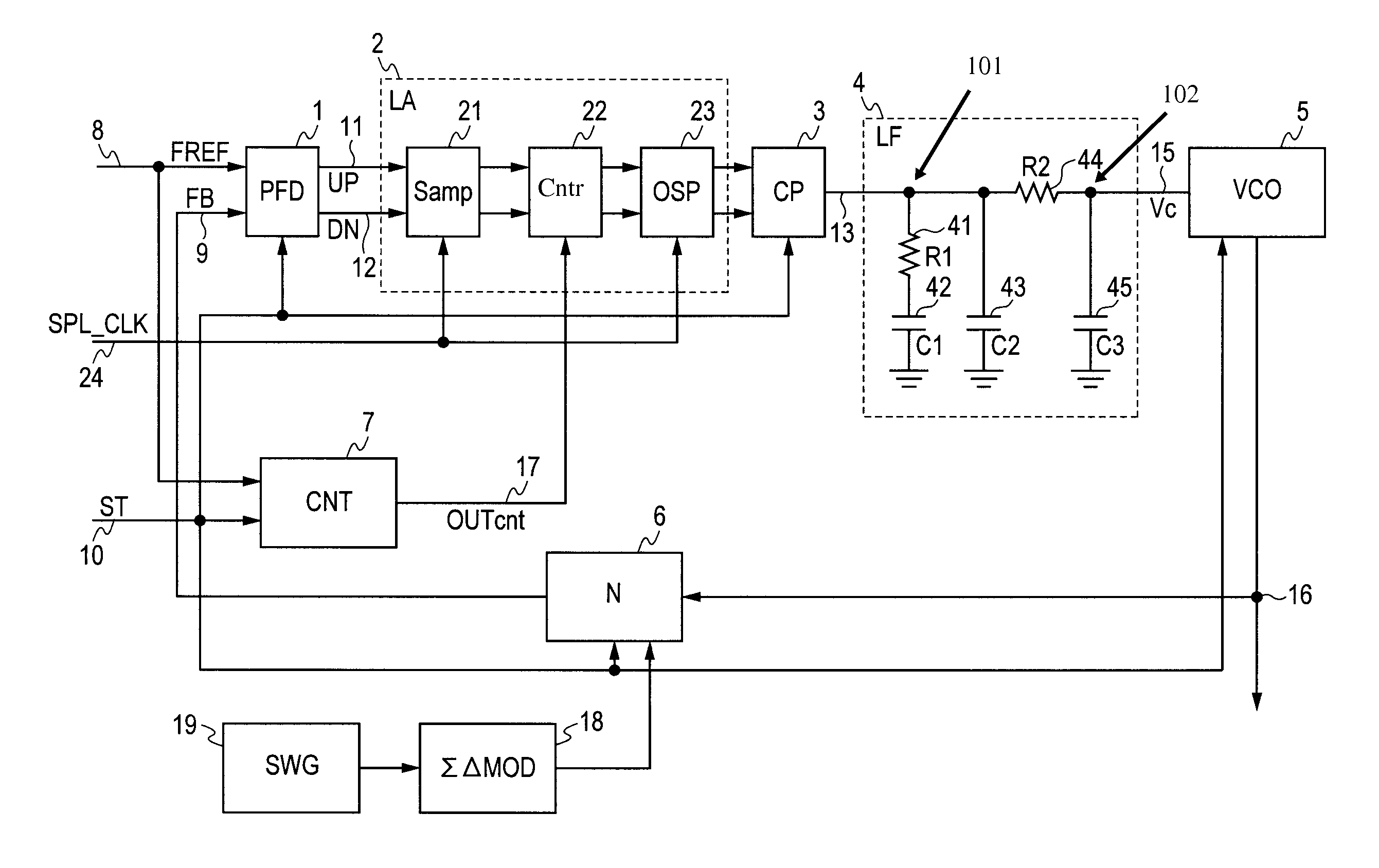
[0094]FIG. 1 is a diagram for describing a configuration of a PLL circuit onchip-integrated into a semiconductor integrated circuit according to a first embodiment of the present invention.
[0095]The onchip-integrated PLL circuit according to the first embodiment of the present invention shown in FIG. 1 is comprised of a phase frequency comparator (PFD) 1, a loop attenuator (LA) 2, a charge pump (CP) 3, a loop filter (LF) 4, a voltage controlled oscillator (VCO) 5, a divider (N) 6 and a controller (CNT) 7. The loop attenuator (LA) 2 includes a sampling circuit (Samp) 21, a counter (Cntr) 22 and a one-shot pulse generator (OSP) 23.
[0096]The phase frequency comparator (PFD) 1 outputs a first output signal (UP) 11 and a second output signal (DN) 12 as phase-compared output signals with a reference signal (FREF) 8 and a feedback signal (FB) 9 as input signals. When the phase of the feedback signal (FB) 9 lags the phase of the reference signal (FREF) 8, a diffe...
second embodiment
Configuration of Fractional PLL Circuit
[0231]FIG. 10 is a diagram for describing a configuration of a PLL circuit on-chip integrated into a semiconductor integrated circuit according to a second embodiment of the present invention.
[0232]The PLL circuit according to the second embodiment of the present invention shown in FIG. 10 is configured as a fractional PLL circuit that configures a spread spectrum clock generator (SSCG) used in a serial ATA interface unit.
[0233]The PLL circuit according to the second embodiment of the present invention shown in FIG. 10 is different from the PLL circuit according to the first embodiment of the present invention shown in FIG. 1 in that a signal waveform generator (SWG) 19 and a modulator (ΣΔMOD) 18 are added to the PLL circuit of FIG. 1.
[0234]The signal waveform generator (SWG) 19 generates a modulating signal and outputs it to the modulator (ΣΔMOD) 18. The modulator (ΣΔMOD) 18 converts the modulating signal to a discrete value as an instantaneou...
further embodiment
Recording and Reproducing Unit
[0240]FIG. 13 is a diagram showing a configuration of a recording and reproducing unit 34 according to a further embodiment of the present invention, which is coupled to a host computer as a peripheral device.
[0241]In the recording and reproducing unit 34 of FIG. 13, the on-chip integrated PLL circuit according to the first embodiment of the present invention shown in FIG. 1 has been adopted in a write strategy PLL circuit (WSPLL) 46 and a reference clock generation PLL circuit (MCKPLL) 51 that generates a reference clock CLK.
[0242]In FIG. 13, an optical disc device is comprised of an optical disc 29, an optical pick-up 30, a semiconductor integrated circuit 31 and a crystal oscillator 33 which provides a reference signal. The optical disc device is coupled to a host computer (HOST) 32 by a serial ATAPI system. Incidentally, ATAPI is an abbreviation of Advanced Technology Attachment Peripheral Interface.
[0243]The optical pick-up 30 applies a light beam ...
PUM
 Abstract
Description
Claims
Application Information
 - R&D
- Intellectual Property
- Life Sciences
- Materials
- Tech Scout
- Unparalleled Data Quality
- Higher Quality Content
- 60% Fewer Hallucinations
Browse by: Latest US Patents, China's latest patents, Technical Efficacy Thesaurus, Application Domain, Technology Topic, Popular Technical Reports.
© 2025 PatSnap. All rights reserved.Legal|Privacy policy|Modern Slavery Act Transparency Statement|Sitemap|About US| Contact US: help@patsnap.com