Nonvolatile logic circuit
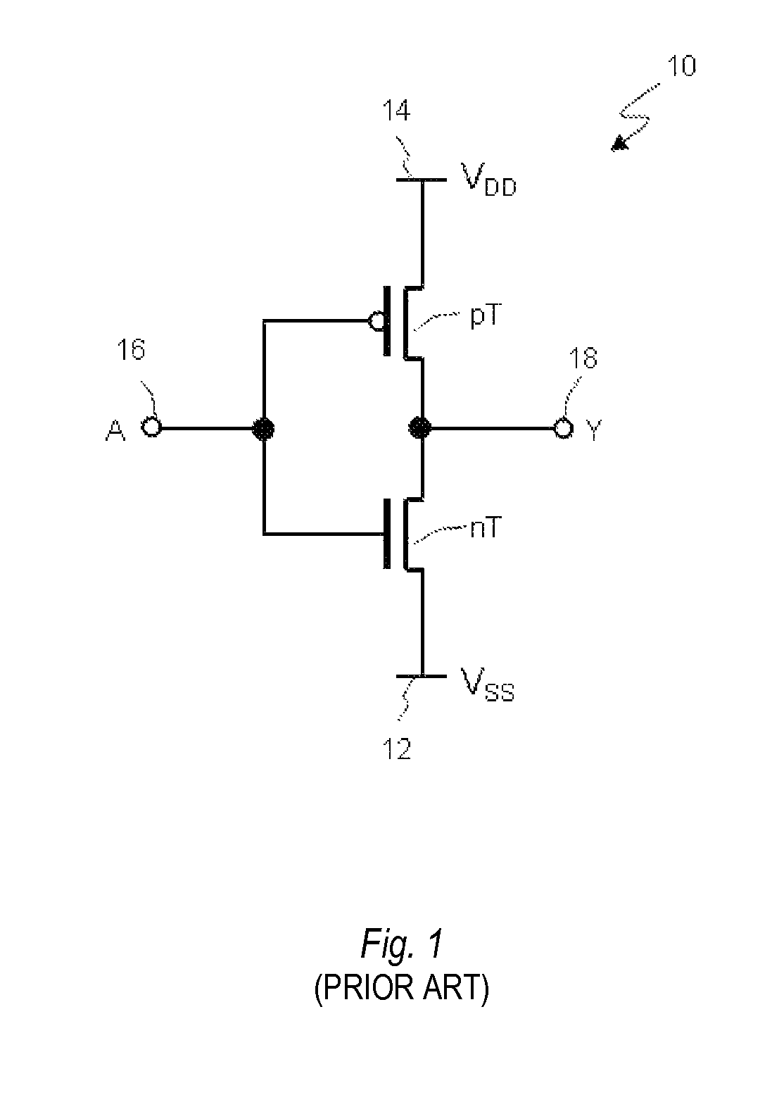
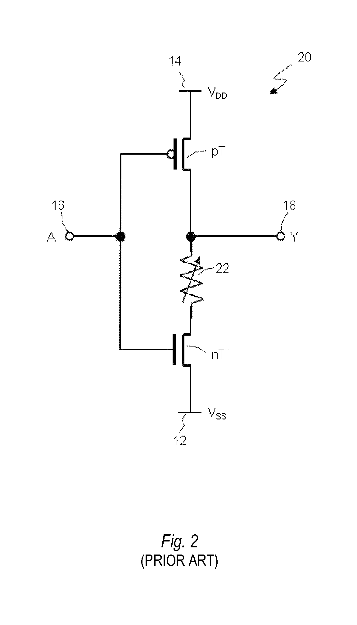
a logic circuit and non-volatile technology, applied in the field of non-volatile logic circuits, can solve the problems of substantial increase of power consumption of the inverter, loss of logic state, volatile state of the cmos inverter b>10/b>,
- Summary
- Abstract
- Description
- Claims
- Application Information
AI Technical Summary
Benefits of technology
Problems solved by technology
Method used
Image
Examples
first embodiment
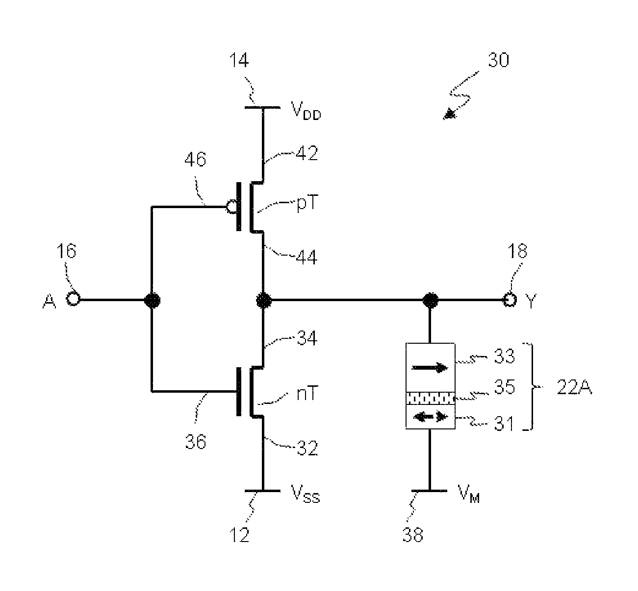
[0035]FIG. 3 illustrates a circuit diagram of a nonvolatile inverter 30 according to a The inverter 30 represents a nonvolatile logic circuit (or gate) that performs a logic function NOT. The inverter 30 comprises a n-channel MOS transistor nT and a complementary p-channel MOS transistor pT connected in series, and a magnetic tunnel junction (MTJ) 22A. A source terminal 32 of the nT transistor is connected to a low voltage source 12 (VSS). Alternatively, a source terminal 42 of the pT transistor is connected to a high voltage source 14 (VDD). Drain terminals 34 and 44 of the nT and pT transistors, respectively, are connected in common and to an output terminal 18. Gate terminals 36 and 46 of the nT and pT transistors, respectively, are connected in common and to an input terminal 16. The MTJ 22A is connected to the output terminal 18 at its first end and to an intermediate (or medium) voltage source 38 (VM) at its second end. There is a following relation between potentials of the ...
second embodiment
[0047]FIGS. 6A and 6B show an nonvolatile logic circuit 60 performing a buffer function according to a Similar to the nonvolatile inverter 30 disclosed above (FIG. 3), the nonvolatile buffer 60 utilizes CMOS technology with one n-channel and one p-channel transistor nT and pT, respectively, connected in series. A source terminal 32 of the transistor nT is connected to a low voltage source 32 (VSS), and a source terminal 42 of the pT transistor is connected to a high voltage source 14 (VDD). Gate terminals 36 and 46 of the transistors nT and pT, respectively, are connected in common and to an input terminal 16. Similarly, drain terminals 34 and 44 of the transistors nT and pT, respectively, are connected in common and to an output terminal 18. A MTJ 22B is connected to the output terminal 18 at its first end and to an intermediate voltage source 38 (VM) at its second end. More specifically, a pinned layer 33 of the MTJ 22B is disposed adjacent the voltage source 38, and a free layer...
fourth embodiment
[0060]FIG. 9 shows a circuit diagram of a 2-input nonvolatile logic circuit 90 according to a The logic circuit 90 performs a logic function AND. The circuit 90 has a similar circuit diagram to that of the nonvolatile logic circuit 80 shown in FIG. 8 but comprises a MTJ 22B, wherein the free layer 31 is disposed adjacent the output terminal 18 and the pinned layer 33 is disposed adjacent the intermediate voltage source 38. A reversed position of the free 31 layer relatively to the output terminal 18 in the logic circuit 90 compared to that in the logic circuit 80 results in an reversed polarity of the output signal Y when similar combinations of the signals A and B appear at the input terminals 16A and 16B. A truth table of the nonvolatile logic circuit 90 performing AND function is given in Table 4.
[0061]
TABLE 4InputInputMTJOutputABResistanceY00RP001RP010RP011 RAP1
PUM
 Abstract
Description
Claims
Application Information
 - R&D
- Intellectual Property
- Life Sciences
- Materials
- Tech Scout
- Unparalleled Data Quality
- Higher Quality Content
- 60% Fewer Hallucinations
Browse by: Latest US Patents, China's latest patents, Technical Efficacy Thesaurus, Application Domain, Technology Topic, Popular Technical Reports.
© 2025 PatSnap. All rights reserved.Legal|Privacy policy|Modern Slavery Act Transparency Statement|Sitemap|About US| Contact US: help@patsnap.com


