Light emitting device having inorganic luminescent particles in inorganic hole transport material

a technology of inorganic luminescent particles and light emitting devices, which is applied in the direction of discharge tubes/lamp details, discharge tubes luminescnet screens, natural mineral layered products, etc., can solve the problems of limited use of el devices, insufficient brightness and efficiency of inorganic el devices using inorganic materials as luminescent materials, and insufficient long-term reliability of el devices for display devices. , to achieve the effect of high brightness, low voltage and high efficiency

Inactive Publication Date: 2012-11-06
PANASONIC CORP
View PDF24 Cites 1 Cited by
  • Summary
  • Abstract
  • Description
  • Claims
  • Application Information

AI Technical Summary

Benefits of technology

[0009]The present invention has been achieved to solve the above-mentioned problems. An object of the present invention is to provide a light emitting device that easily can be made planar and can achieve high brightness, high efficiency and light emission at a low voltage by efficiently providing holes and electrons to a particulate luminescent material. Another object of the present invention is to provide a display device using such a light emitting device.
[0012]The present invention can provide a light emitting device that easily can be made planar and that can achieve high brightness, high efficiency and light emission at a low voltage. Since the display device of the present invention includes such a light emitting device, the display device can achieve high brightness, high efficiency and low voltage drive capability.

Problems solved by technology

However, EL devices using organic materials as a luminescent material are insufficient in long-term reliability for the use in display devices.
Furthermore, inorganic EL devices using inorganic materials as a luminescent material are insufficient in brightness and efficiency.
Because of these and other reasons, the use of the EL devices is limited to specific applications.
However, the LEDs are put in practical use only as a point light source, and use of the LEDs in display devices is limited to a specific application such as a light source for a backlight in liquid crystal displays.
However, gallium nitride (GaN), a typical example of the group 13 nitride semiconductors, has the disadvantage of a substrate material being restricted due to a difference in a lattice constant and a difference in a thermal expansion coefficient.
That is, the application to large-area display devices is still difficult in view of performance and in view of cost.
The conventional techniques mentioned above have the advantage of reducing the mismatch with a substrate (such mismatch is observed in the LEDs) and have the advantage of ease of enlargement, however, they have not reached a sufficient level as a display device in practical use in view of brightness and light emission efficiency.

Method used


Image

  • Light emitting device having inorganic luminescent particles in inorganic hole transport material
  • Light emitting device having inorganic luminescent particles in inorganic hole transport material
  • Light emitting device having inorganic luminescent particles in inorganic hole transport material

Examples


example 1

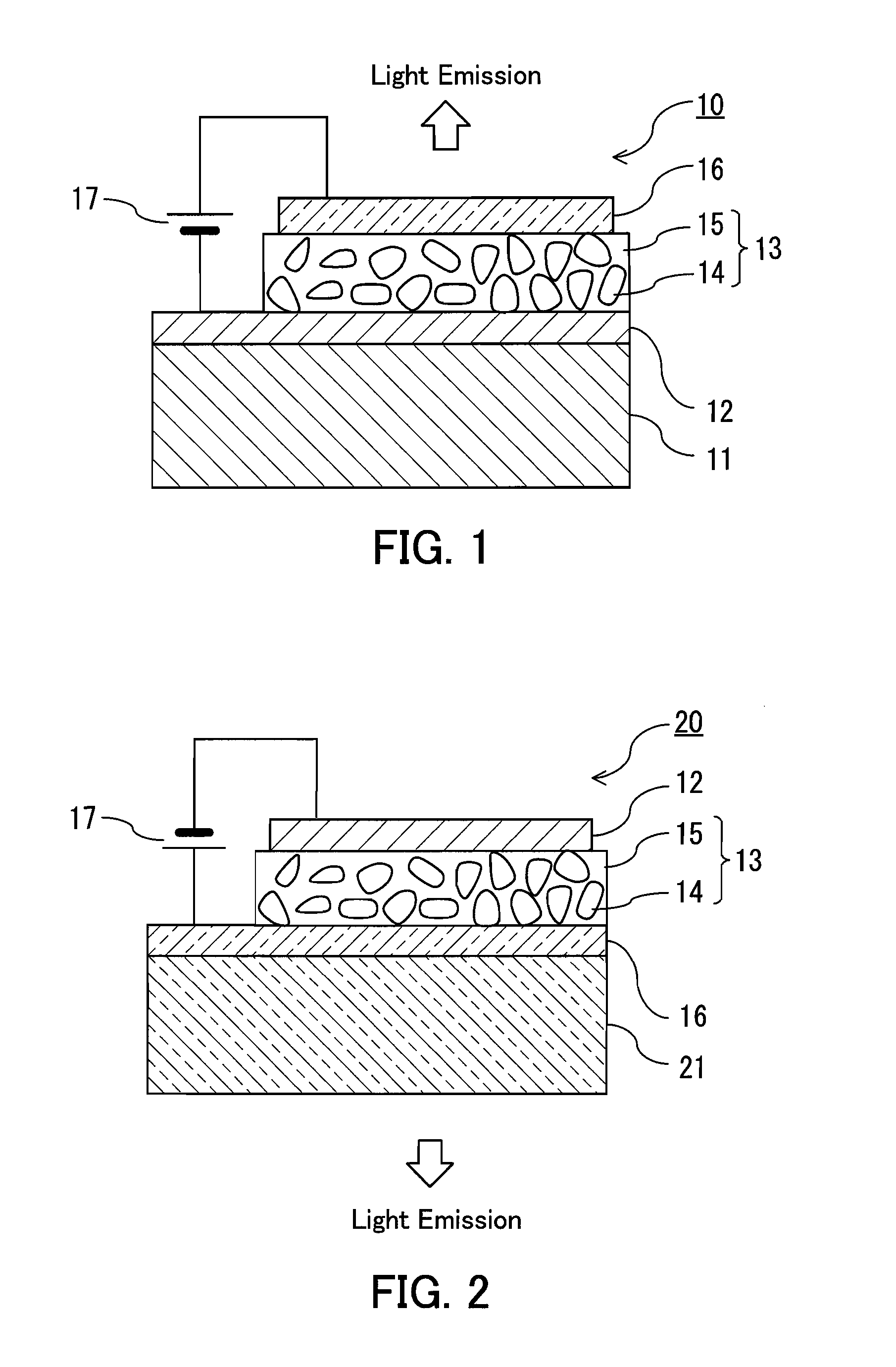
[0061]A light emitting device having the same structure as the light emitting device 10 shown in FIG. 1 was fabricated as a light emitting device of Example 1.

[0062]First, Ga2O3 was allowed to react in an ammonia atmosphere at 1000° C. for 3 hours, thereby preparing GaN particles as luminescent particles. The average particle diameter of the resultant GaN particles was 2 μm.

[0063]Next, the GaN particles thus obtained and a paste containing SiC fine particles (average particle diameter: 5 nm) used as an inorganic hole transport material were kneaded at a volume ratio of 1:1. The paste was a mixture in which the SiC fine particles and a binder (“EL binder” made by Saitama Yakuhin Co. Ltd.) were mixed at the volume ratio of 1:1. The light emitting layer was formed using the kneaded mixture in which the GaN particles were dispersed. Specifically, the light emitting layer was formed by applying the kneaded mixture of the GaN particles and the SiC fine particles on an ITO electrode of a g...

example 2

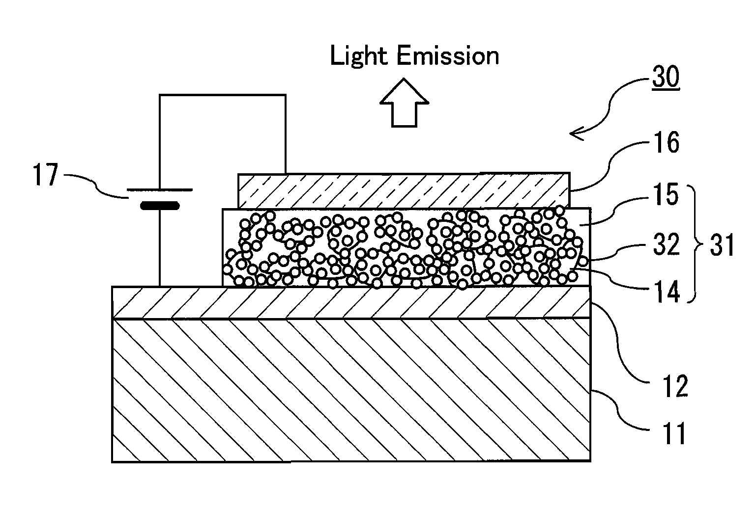
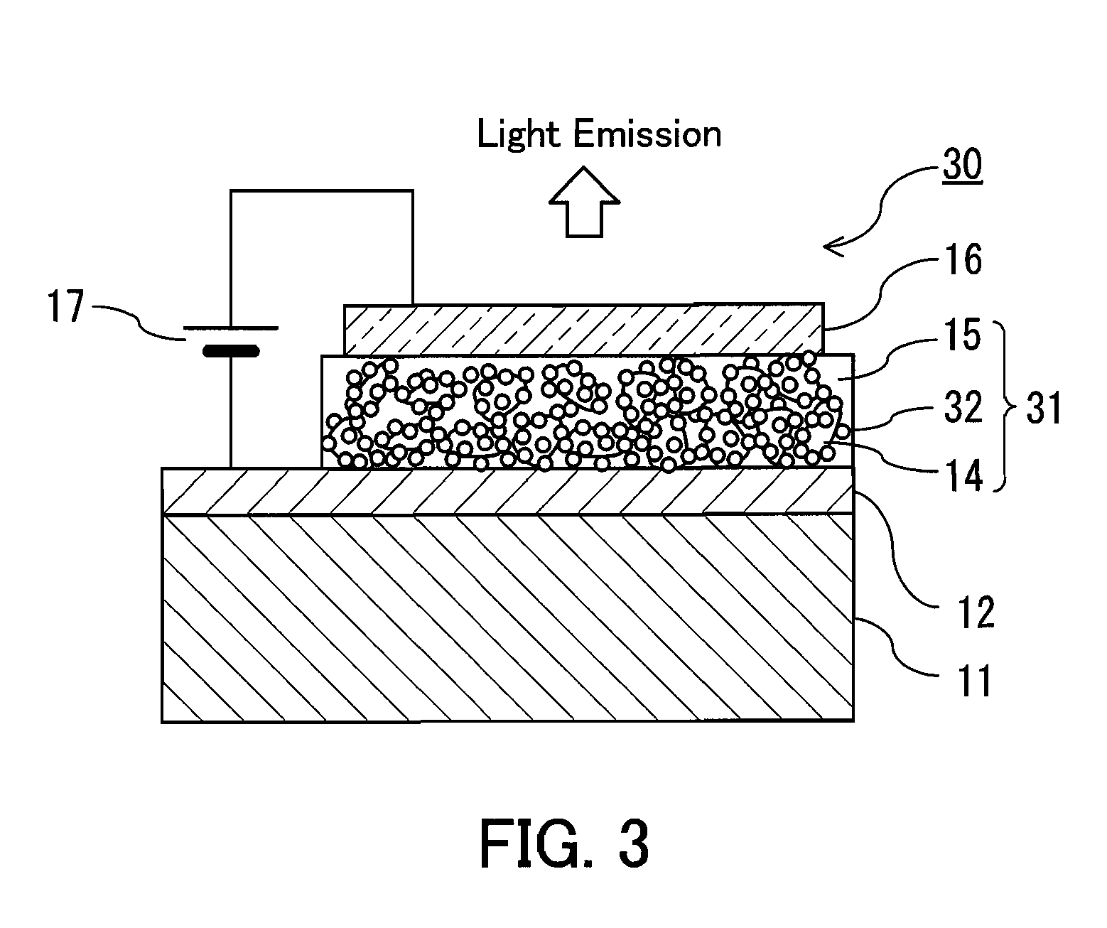
[0065]A light emitting device of Example 2 having the same structure as the light emitting device 30 shown in FIG. 3 was fabricated.

[0066]First, Ga2O3 was allowed to react in an ammonia atmosphere at 1000° C. for 3 hours, thereby preparing GaN particles as luminescent particles. The average particle diameter of the resultant GaN particles was 2 μm. An ITO nano paste (“X-105” made by SUMITOMO METAL MINING CO., LTD., average particle diameter of ITO fine particles: 50 nm) was used for the conductive fine particles. The ITO nano paste and the GaN particles were kneaded at 1:1 (volume ratio) so that the conductive fine particles made of ITO were adhered to the surfaces of the GaN particles.

[0067]Next, the resultant GaN particles to which the conductive fine particles were adhered and a paste containing, as a main component, SiC fine particles (average particle diameter: 5 nm) used as an inorganic hole transport material were kneaded at a volume ratio of 1:1. The paste was a mixture of t...

example 3

[0068]GaN particles to which the conductive fine particles were adhered were prepared in the same manner as described in Example 2. Next, the GaN particles were dispersed on a surface of a Si substrate except for an electrode pad bonding region. At that time, detachment of the GaN particles from the substrate was prevented using the planarization material (inorganic SOG, “HSG-255” made by Hitachi Chemical Co., Ltd.) that is generally used for forming interlayer dielectric films. Next, Se was evaporated on the resultant GaN particles layer to constitute a matrix portion (inorganic hole transport material) made of a-Se between the GaN particles, thereby forming a light emitting layer. Next, an ITO electrode was formed on the light emitting layer using a sputtering method. Thus, a light emitting device was obtained. When a direct current voltage was applied to the resultant device in the same manner as Example 1 to evaluate its light emission performance, the device emitted light at 11...


PUM

PropertyMeasurementUnit
particle diameteraaaaaaaaaa
diameteraaaaaaaaaa

Abstract

A light emitting device (10) of the present invention includes luminescent particles (14) and a pair of electrodes (12, 16) for injecting an electric current into the luminescent particles (14). An inorganic hole transport material (15) is disposed between the electrodes (12, 16). The luminescent particles (14) are dispersed in the inorganic hole transport material (15). Conductive fine particles may be adhered to at least a part of the surfaces of the luminescent particles (14) for the purpose of achieving further high brightness and high efficiency.

Description

TECHNICAL FIELD[0001]The present invention relates to light emitting devices and display devices using the same.BACKGROUND ART[0002]In recent years, many kinds of flat type display devices have been proposed and are put in practical use. Among them, display devices using electroluminescence (hereinafter abbreviated as “EL”) devices as a light emitting device of the surface-emitting type have received attention because of their usefulness. The EL devices are used as a backlight in liquid crystal displays or used for matrix type display devices in which the EL devices themselves are arranged in an array. For example, matrix type display devices using EL devices have good features such as self-luminosity, excellent visibility, wide view angle, and fast response. However, EL devices using organic materials as a luminescent material are insufficient in long-term reliability for the use in display devices. Furthermore, inorganic EL devices using inorganic materials as a luminescent materi...

Claims


Application Information

Patent Timeline
Patent Type & Authority Patents(United States)
IPC IPC(8): H05B33/02
CPCH05B33/145H05B33/20
Inventor ONO, MASAYUKINASU, SHOGOSATOH, EIICHITANIGUCHI, REIKOSHIMAMURA, TAKAYUKIODAGIRI, MASARU
Owner PANASONIC CORP
Why Eureka
Try Eureka