
Epitaxial film, piezoelectric element, ferroelectric element, manufacturing methods of the same, and liquid discharge head

a technology of piezoelectric elements and films, applied in the field of piezoelectric/electrostrictive device material selection, device material selection, printing, etc., can solve the problems of in-plane composition fluctuation, difficult to reduce the content of y in the resultant film, and inconvenient forming films having a large area, etc., to achieve excellent crystal orientation, excellent characteristics, and uniform composition

Active Publication Date: 2012-06-12
CANON KK +1
View PDF12 Cites 0 Cited by
  • Summary
  • Abstract
  • Description
  • Claims
  • Application Information

AI Technical Summary

Benefits of technology

The present invention provides a method for manufacturing a large-area epitaxial film with a uniform composition and excellent crystal orientation on an Si substrate. The method involves heating the substrate and forming a SiO2 layer with a specific thickness on the surface of the substrate. The epitaxial film is then formed using a metal target represented by a specific composition formula. The resulting epitaxial film can be used as a buffer layer on an Si substrate to create a single-oriented crystal structure and excellent characteristics. The invention also provides a piezoelectric element, a ferroelectric element, and a liquid discharge head using the epitaxial film as a buffer layer. The epitaxial film has a uniform composition, a single oriented crystal structure, and a large area, making it ideal for use in these applications. The manufacturing method is simple and efficient, and the resulting elements have excellent performance.

Problems solved by technology

However, in the buffer layer disclosed in Patent Document 1, laminated films having crystal surfaces thereof aligned with the surface of the substrate are formed by an electronic beam evaporation process, and this is not suitable for forming films having a large area.
In addition, when the film having a large area of 3 inches or more is formed, there is a problem that fluctuations of an in-plane composition increase.
It is difficult to reduce the content of Y in the resultant film.
In general, when the film is formed by a sputtering process, a composition of a target is not reflected in that of the epitaxial film as it is, and it is very difficult to find an optimum composition of the target for obtaining the epitaxial film having a targeted composition.

Method used


Image

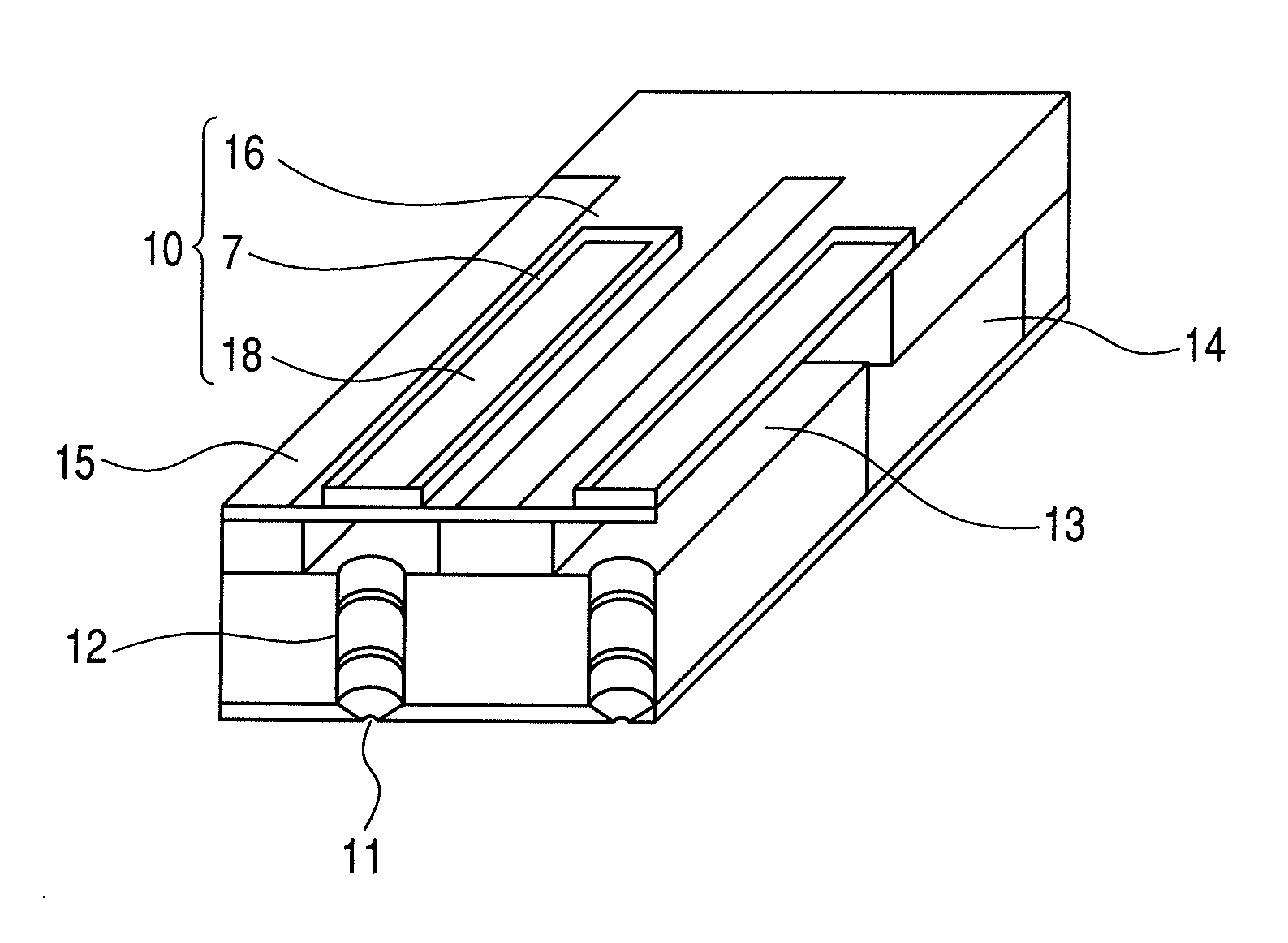
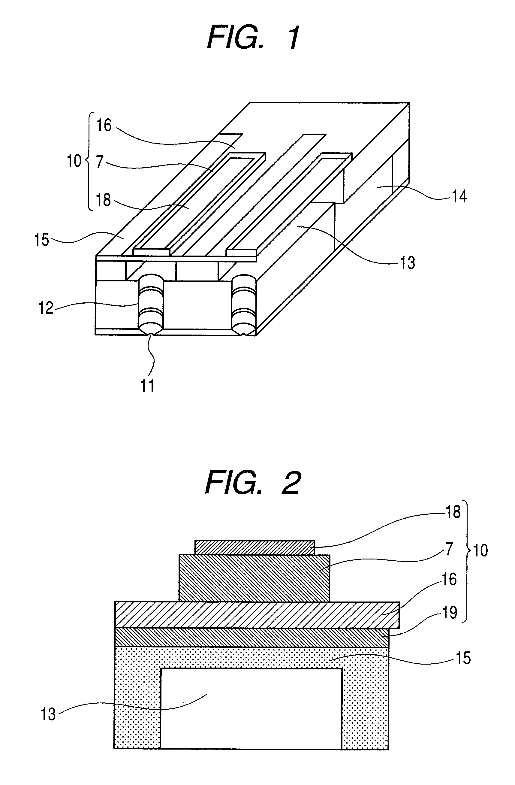
  • Epitaxial film, piezoelectric element, ferroelectric element, manufacturing methods of the same, and liquid discharge head
  • Epitaxial film, piezoelectric element, ferroelectric element, manufacturing methods of the same, and liquid discharge head
  • Epitaxial film, piezoelectric element, ferroelectric element, manufacturing methods of the same, and liquid discharge head

Examples


example 1

(Preparation of Epitaxial Film)

[0068]An epitaxial film was formed on an Si (100) single crystal substrate by use of an alloy target of 0.11Y-0.89Zr containing Y and Zr components and prepared by a vacuum melting process as follows.

(Initial Layer Film Formation)

[0069]A heating temperature was set to 624° C., and the substrate was heated for 30 minutes. After elapse of 30 minutes, an Ar gas was introduced, and a sputtering power supply was turned on to start pre-sputtering. At this time, a gas pressure and a sputtering power were set to 0.5 Pa and 2.96 W / cm2, respectively. The pre-sputtering was performed for ten minutes, and then sputtering was performed for four seconds to form an initial layer.

(Oxide Layer Film Formation)

[0070]The initial layer was formed, and then the sputtering power supply was turned off to introduce an O2 gas. The sputtering power supply was turned on again to start the pre-sputtering. At this time, a gas pressure and a sputtering power were set to 0.3 Pa and 5...

example 2

(Preparation of Epitaxial Film)

[0078]An epitaxial film was formed on an Si (100) single crystal substrate by use of an alloy target of 0.14Y-0.86Zr containing Y and Zr components as follows.

(Initial Layer Film Formation)

[0079]A heating temperature was set to 635° C., and the substrate was heated for 30 minutes. After elapse of 30 minutes, an Ar gas was introduced, and a sputtering power supply was turned on to start pre-sputtering. At this time, a gas pressure and a sputtering power were set to 0.3 Pa and 2.96 W / cm2, respectively. The pre-sputtering was performed for ten minutes, and then sputtering was performed for four seconds to form an initial layer.

(Oxide Layer Film Formation)

[0080]The initial layer was formed, and then the sputtering power supply was turned off to introduce an O2 gas. The sputtering power supply was turned on again to start the pre-sputtering. At this time, a gas pressure and a sputtering power were set to 0.3 Pa and 5.92 W / cm2, respectively, and a mixture ga...

example 3

(Preparation of Epitaxial Film)

[0085]An epitaxial film was formed on an Si (100) single crystal substrate by use of an alloy target of 0.07Y-0.993Zr containing Y and Zr components as follows.

(Initial Layer Film Formation)

[0086]A heating temperature was set to 600° C., and the substrate was heated for 25 minutes. After elapse of 35 minutes, an Ar gas was introduced, and a sputtering power supply was turned on to start pre-sputtering. At this time, a gas pressure and a sputtering power were set to 0.5 Pa and 2.96 W / cm2, respectively. The pre-sputtering was performed for ten minutes, and then sputtering was performed for four seconds to form an initial layer.

(Oxide Layer Film Formation)

[0087]The initial layer was formed, and then the sputtering power supply was turned off to introduce an O2 gas. The sputtering power supply was turned on again to start the pre-sputtering. At this time, a gas pressure and a sputtering power were set to 0.5 Pa and 5.92 W / cm2, respectively, and a mixture g...


PUM

PropertyMeasurementUnit
thicknessaaaaaaaaaa
lattice constantaaaaaaaaaa
thicknessaaaaaaaaaa

Abstract

There are disclosed an epitaxial film, comprising: heating an Si substrate provided with an SiO2 layer with a film thickness of 1.0 nm or more to 10 nm or less on a surface of the substrate; andforming on the SiO2 layer by use of a metal target represented by the following composition formula:yA(1−y)B  (1),in which A is one or more elements selected from the group consisting of rare earth elements including Y and Sc, B is Zr, and y is a numeric value of 0.03 or more to 0.20 or less, the epitaxial film represented by the following composition formula:xA2O3−(1−x)BO2  (2),in which A and B are respectively same elements as A and B of the composition formula (1), and x is a numeric value of 0.010 or more to 0.035 or less.

Description

TECHNICAL FIELD[0001]The present invention relates to an epitaxial film preferable for a buffer layer for preparing an electronic device to be formed on an Si substrate, a piezoelectric element and a ferroelectric element using the epitaxial film, manufacturing methods thereof, and a liquid discharge head.BACKGROUND ART[0002]An Si substrate which is a semiconductor single crystal substrate has excellent crystallinity, and an area of the substrate can be enlarged, so that the substrate is suitable as a substrate to prepare an electronic device, and is used for a general purpose. Examples of the electronic device to be laminated and prepared on the Si substrate include a dielectric device, a piezoelectric device, a ferroelectric device and a pyroelectric device. A buffer layer as an underlayer to be formed on the Si substrate in order to improve a crystal structure of the device has been investigated.[0003]In the buffer layer, as a material excellent in lattice matching with Si crysta...

Claims


Application Information

Patent Timeline
Patent Type & Authority Patents(United States)
IPC IPC(8): H01L21/31B41J2/045B41J2/055B41J2/135B41J2/14B41J2/16H01L21/316H01L41/09H01L41/18H01L41/187H01L41/22H01L41/316
CPCH01L41/0815H01L41/0973H01L41/319H10N30/2047H10N30/079H10N30/708
Inventor HAYASHI, JUMPEIMATSUDA, TAKANORIFUKUI, TETSUROFUNAKUBO, HIROSHI
Owner CANON KK
Learn More